 ALLPCB


Designing vias for a 14-layer PCB can be a complex task, but it’s crucial for ensuring signal integrity, power distribution, and overall board performance. In this comprehensive guide, we’ll explore everything you need to know about via design in 14-layer PCBs, including 14-layer PCB via types, via-in-pad design, blind and buried vias, high-density PCB vias, and microvia design. Whether you’re an experienced engineer or just starting with multilayer boards, this guide will provide actionable insights to help you optimize your designs.
Why Via Design Matters in 14-Layer PCBs
A 14-layer PCB is a high-density multilayer board often used in advanced electronics like telecommunications equipment, medical devices, and high-speed computing systems. With so many layers, vias—small conductive holes that connect different layers—play a critical role in maintaining electrical connections and signal quality. Poor via design can lead to issues like signal loss, crosstalk, or even board failure. By understanding the different via types and design techniques, you can create reliable and efficient 14-layer PCBs.
Understanding the Basics of Vias in Multilayer PCBs
Vias are essentially pathways that allow electrical signals and power to travel between layers of a PCB. In a 14-layer PCB, where space is limited and signal paths are complex, vias must be carefully designed to avoid interference and maintain performance. Let’s break down the key aspects of via design specific to such multilayer boards.
What Are Vias and Why Are They Important?
Vias are small plated holes that create electrical connections between layers. In a 14-layer PCB, they help route signals and power through multiple layers without taking up excessive space on the surface. They are essential for high-density designs where components are packed tightly, and routing must be efficient. Without well-designed vias, you risk signal degradation, increased impedance, or even short circuits.
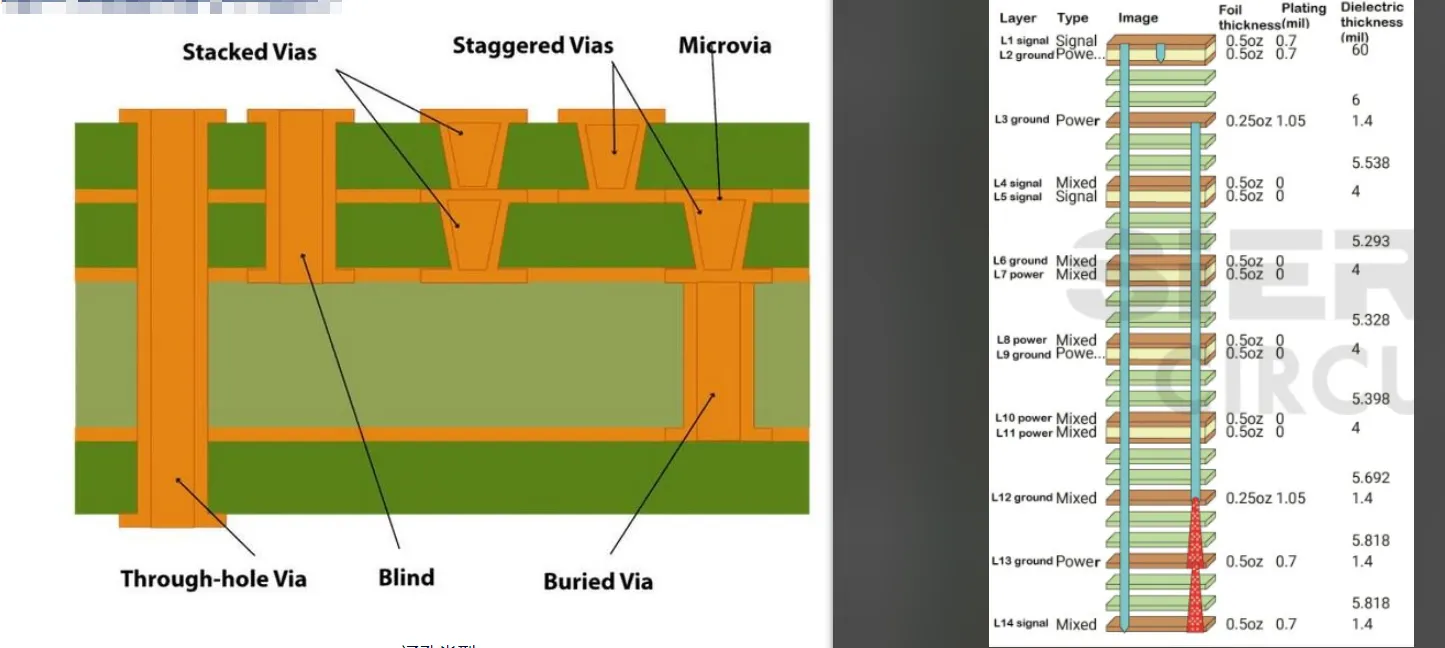
Types of Vias in 14-Layer PCBs
In 14-layer PCB designs, several via types are used depending on the specific needs of the board. Below, we’ll explore the most common 14-layer PCB via types and their applications.
1. Through-Hole Vias
Through-hole vias extend through all layers of the PCB, from the top to the bottom. They are the simplest and most cost-effective via type but can take up valuable space in a 14-layer PCB. They are often used for power and ground connections where signal routing isn’t a primary concern. However, in high-density designs, their use is minimized to save space.
2. Blind Vias
Blind vias connect an outer layer to one or more inner layers but do not extend through the entire board. For instance, a blind via might connect layer 1 to layer 3 without reaching layer 14. These vias are ideal for high-density PCB vias as they free up space on other layers. However, they are more expensive to manufacture due to the precision required.
3. Buried Vias
Buried vias connect internal layers without reaching the outer surfaces. For example, a buried via might link layer 5 to layer 8 in a 14-layer PCB. These are perfect for complex inner-layer routing and are often used alongside blind vias in high-density designs. Like blind vias, they increase manufacturing costs but are essential for compact layouts.
4. Microvias
Microvias are tiny vias, typically less than 0.15 mm in diameter, used in high-density interconnect (HDI) designs. They are often employed in 14-layer PCBs to connect closely spaced layers, such as layer 1 to layer 2. Microvia design is critical for modern electronics where space is at a premium. They are usually created using laser drilling for precision, and their small size helps reduce signal path length, improving performance at high frequencies (e.g., above 1 GHz).
Key Considerations for Via Design in 14-Layer PCBs
Designing vias for a 14-layer PCB involves balancing performance, cost, and manufacturability. Below are the key factors to consider when planning your via layout.
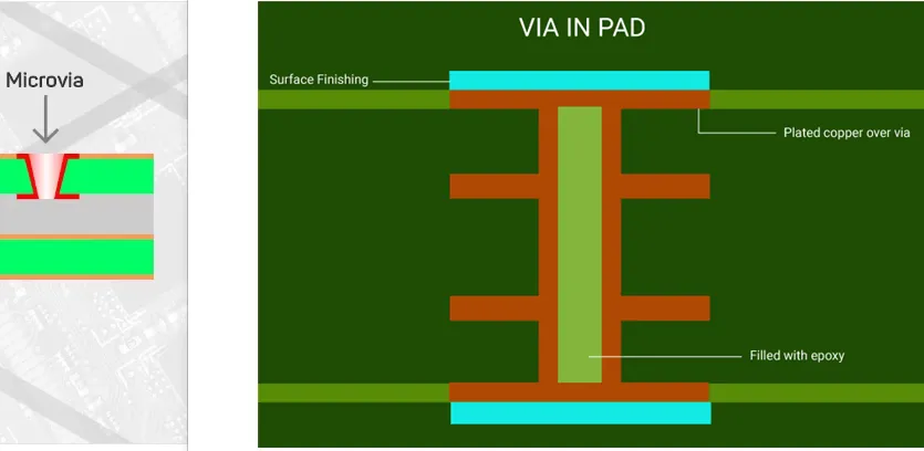
1. Via-In-Pad Design
Via-in-pad design involves placing a via directly within the pad of a surface-mount component, such as a BGA (Ball Grid Array). This technique is often used in 14-layer PCBs to save space and improve routing density. However, it requires careful planning to avoid soldering issues. For instance, vias must be filled or capped to prevent solder from wicking into the hole during assembly. Via-in-pad design is particularly useful for high-density PCB vias where traditional routing isn’t feasible.
A typical via-in-pad might have a diameter of 0.2 mm and be filled with conductive epoxy to ensure a flat surface for soldering. This approach reduces the risk of voids and improves thermal dissipation, which is critical for components dissipating heat at rates of 2-5 W.
2. Blind and Buried Vias for Space Efficiency
As mentioned earlier, blind and buried vias are indispensable for 14-layer PCBs with tight space constraints. By limiting via exposure to specific layers, you can maximize routing space on other layers. For example, in a design with high-speed signals on layers 1 and 14, blind vias can connect these layers to inner signal layers without cluttering the board’s surface. However, keep in mind that using blind and buried vias can increase fabrication costs by 20-30% due to the need for sequential lamination and precise drilling.
3. High-Density PCB Vias and Routing Challenges
In a 14-layer PCB, high-density PCB vias are often necessary to accommodate numerous connections in a small area. This is especially true for designs with fine-pitch components (e.g., 0.5 mm pitch BGAs). To manage high-density routing, consider using microvias and staggered via patterns to avoid overlap and reduce crosstalk. Additionally, ensure that via spacing adheres to manufacturer guidelines—typically at least 0.3 mm between vias—to prevent drilling errors and maintain structural integrity.
4. Microvia Design for High-Speed Signals
Microvia design is a game-changer for high-speed applications in 14-layer PCBs. Their small size and short length minimize signal delay and inductance, which is vital for maintaining signal integrity at frequencies above 500 MHz. When designing microvias, aim for an aspect ratio (depth-to-diameter) of 0.75:1 or lower to ensure reliable plating. For instance, a microvia with a depth of 0.1 mm should have a diameter of at least 0.13 mm. Stacked microvias, where multiple microvias are placed on top of each other, can also be used to connect more layers in HDI designs.
Best Practices for Via Design in 14-Layer PCBs
To achieve optimal performance in your 14-layer PCB, follow these best practices for via design. These tips are based on industry standards and practical experience with multilayer boards.
1. Minimize Via Count Where Possible
While vias are essential, too many can clutter your design and increase manufacturing complexity. Use layer planning to reduce the number of vias by routing signals on adjacent layers whenever possible. For example, if a signal can travel from layer 2 to layer 3 without a via, prioritize that path to avoid unnecessary drilling.
2. Optimize Via Placement for Signal Integrity
Place vias strategically to minimize signal path length and avoid interference. For high-speed signals, keep vias away from critical traces or use back-drilling to remove unused via stubs, which can cause reflections at frequencies above 1 GHz. A via stub of just 0.5 mm can introduce significant signal distortion in a 5 Gbps design.
3. Use Proper Via Sizes and Annular Rings
Choose via sizes based on current-carrying capacity and manufacturing capabilities. For power vias, a diameter of 0.4-0.6 mm is often sufficient to handle currents up to 2 A. Signal vias can be smaller, around 0.2-0.3 mm. Ensure that the annular ring (the copper pad around the via) is at least 0.1 mm wide to maintain a strong connection during drilling and plating.
4. Consider Thermal Management
In 14-layer PCBs, thermal vias can help dissipate heat from high-power components. Place thermal vias under components like power ICs to transfer heat to inner copper planes. A grid of 0.3 mm vias spaced 1.2 mm apart can effectively reduce thermal resistance by up to 50% in some designs.
Common Challenges in 14-Layer PCB Via Design
Designing vias for a 14-layer PCB comes with unique challenges. Here are some common issues and how to address them.
1. Manufacturing Limitations
High-density designs with microvias and blind/buried vias require advanced manufacturing techniques like laser drilling and sequential lamination. Not all fabricators can handle aspect ratios below 0.75:1 for microvias or guarantee alignment for stacked vias. Always check with your manufacturer to confirm their capabilities before finalizing your design.
2. Signal Integrity Issues
In high-speed designs, vias can act as impedance discontinuities, causing signal reflections. To mitigate this, use controlled impedance routing and minimize via transitions for critical signals. For a 50-ohm trace, ensure that the via impedance mismatch is less than 10% to avoid significant signal loss.
3. Cost vs. Performance Trade-Offs
Advanced via types like blind, buried, and microvias improve performance but increase costs. Balance your design needs with budget constraints by using these vias only where necessary. For example, reserve microvias for high-speed signal layers and use through-hole vias for less critical connections.
Tools and Software for Via Design in 14-Layer PCBs
Designing vias for a 14-layer PCB is easier with the right tools. Modern PCB design software offers features like 3D visualization, impedance calculators, and via optimization to streamline the process. Look for software that supports HDI design rules and allows you to define via types, sizes, and stackups. These tools can help you simulate signal integrity and identify potential issues before manufacturing.
Conclusion: Mastering Via Design for 14-Layer PCBs
Via design is a critical aspect of creating reliable and high-performing 14-layer PCBs. By understanding the different 14-layer PCB via types, mastering via-in-pad design, leveraging blind and buried vias, optimizing high-density PCB vias, and refining microvia design, you can tackle even the most complex multilayer projects. Follow the best practices outlined in this guide, and always consider signal integrity, thermal management, and manufacturing constraints in your designs.
With careful planning and the right approach, your 14-layer PCB can achieve exceptional performance for advanced applications. Keep experimenting with different via configurations to find the perfect balance for your specific needs, and stay updated on the latest design techniques to stay ahead in the fast-evolving world of PCB technology.


