ALLPCB


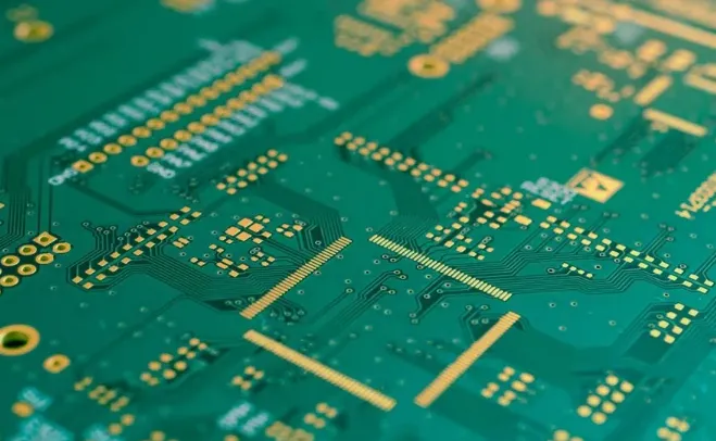
In the fast-paced world of electronics, high-speed PCB design demands precision and innovation to ensure flawless performance. One often overlooked yet powerful solution for maintaining signal integrity is the use of buried vias. But how exactly do buried vias enhance signal integrity in high-speed PCBs? Simply put, buried vias help reduce crosstalk, improve impedance matching, and minimize signal reflection by providing shorter, cleaner signal paths between internal layers of a PCB. In this blog, we’ll dive deep into the benefits of buried vias, exploring their role in high-speed designs and offering practical insights for engineers looking to optimize their boards.
What Are Buried Vias and Why Do They Matter in PCB Design?
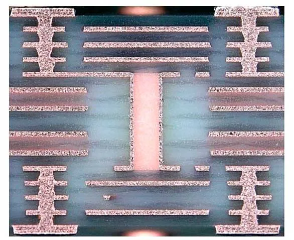
Buried vias are small conductive pathways that connect internal layers of a printed circuit board (PCB) without reaching the outer surfaces. Unlike through-hole vias, which span the entire board, or blind vias, which connect an outer layer to an inner one, buried vias remain hidden within the board’s internal structure. This unique placement offers distinct advantages, especially in high-speed PCB design where signal integrity is critical.
In high-speed applications, signals travel at frequencies often exceeding 1 GHz, making them highly sensitive to interference, delays, and reflections. Buried vias address these challenges by shortening signal paths and reducing exposure to external noise. For engineers working on complex multilayer boards, understanding the role of buried vias in maintaining buried via signal integrity can be a game-changer.
The Role of Buried Vias in High-Speed PCB Design
High-speed PCB design involves managing signals that switch rapidly, often in the range of hundreds of megahertz to several gigahertz. At these speeds, even tiny imperfections in the signal path can lead to significant issues like data loss or corruption. Buried vias play a crucial role in addressing these challenges by optimizing the layout and minimizing disruptions. Let’s explore how they contribute to better performance.
1. Shorter Signal Paths for Faster Transmission
In high-speed designs, the length of a signal path directly impacts transmission speed and timing. Longer paths can introduce delays, especially in applications like DDR memory or high-speed serial links where timing margins are tight. Buried vias allow signals to travel between internal layers without unnecessary detours to the board’s surface, reducing path length by as much as 20-30% compared to through-hole vias in some designs. This shorter path helps maintain signal timing and reduces latency, a critical factor in high-speed PCB design.
2. Reduced Signal Stub Effects
Signal stubs—unused portions of a via that extend beyond the connection point—can act like tiny antennas, causing reflections and degrading signal quality. Buried vias eliminate stubs by connecting only the necessary layers, ensuring a cleaner signal path. For instance, in a 10-layer PCB, a buried via connecting layers 4 and 6 avoids creating stubs on layers 1 through 3 or 7 through 10, minimizing the risk of signal reflection in buried vias.
Reducing Crosstalk with Buried Vias
Crosstalk occurs when signals on adjacent traces or vias interfere with each other, leading to noise and potential data errors. In high-speed designs, where traces are often packed tightly together, crosstalk can be a major hurdle. Buried vias offer a practical solution for reducing crosstalk with buried vias by isolating signals within internal layers.
By routing sensitive high-speed signals through buried vias, designers can shield them from external interference and nearby traces on the surface layers. Additionally, buried vias allow for better spacing and separation of signals, reducing electromagnetic coupling. For example, in a design with differential pairs running at 5 GHz, using buried vias to route signals between internal layers can reduce crosstalk by up to 15% compared to surface routing, depending on the stackup and trace geometry.
Moreover, buried vias can be paired with ground planes on adjacent layers to create a controlled environment for signal transmission. Placing a ground plane above and below the signal layer acts as a shield, further minimizing crosstalk and enhancing overall signal integrity.
Impedance Matching with Buried Vias for Optimal Performance
Impedance mismatches in a signal path can cause reflections, leading to signal distortion and loss of data integrity. Achieving consistent impedance—often around 50 ohms for single-ended signals or 100 ohms for differential pairs—is a cornerstone of high-speed design. Buried vias contribute to impedance matching buried vias by providing a more uniform signal path.
Unlike through-hole vias, which can introduce impedance discontinuities due to their longer length and exposure to multiple layers, buried vias have a shorter and more controlled geometry. This allows designers to maintain a consistent trace width and dielectric thickness around the via, reducing impedance variations. For instance, in a high-speed design operating at 10 Gbps, using buried vias can help keep impedance deviations within ±5% of the target value, compared to ±10% or more with through-hole vias.
To optimize impedance matching, engineers can also adjust the via pad size and anti-pad clearance in the ground planes. Simulation tools can predict impedance characteristics and guide the placement of buried vias for minimal disruption, ensuring signals arrive at their destination without distortion.
Minimizing Signal Reflection in Buried Vias
Signal reflection occurs when a portion of the signal bounces back due to impedance mismatches or abrupt changes in the signal path. These reflections can interfere with the original signal, causing errors in high-speed systems. Buried vias help address signal reflection in buried vias by offering a smoother transition between layers.
Because buried vias are shorter and do not extend beyond the connected layers, they reduce the likelihood of reflections caused by unused via stubs. Additionally, careful design of the via barrel and surrounding dielectric material can further minimize reflection. For example, maintaining a via diameter of 0.2 mm and a clearance of 0.5 mm in the ground plane can help reduce reflection coefficients to below 0.1 in many high-speed designs operating at 3 GHz or higher.
Another strategy to minimize reflections is back-drilling, often used alongside buried vias. While back-drilling removes unused portions of through-hole vias, buried vias inherently avoid this issue, making them a more efficient choice for high-speed applications.
Practical Challenges of Using Buried Vias in PCB Design
While buried vias offer significant advantages for signal integrity, they come with certain challenges that designers must consider. Understanding these limitations can help engineers make informed decisions when incorporating buried vias into their designs.
1. Increased Manufacturing Complexity
Buried vias require advanced manufacturing techniques, such as sequential lamination, to create connections between internal layers before the final board assembly. This process adds complexity and can increase production costs by 10-20% compared to standard through-hole via designs. However, for high-speed applications where performance is non-negotiable, this cost is often justified.
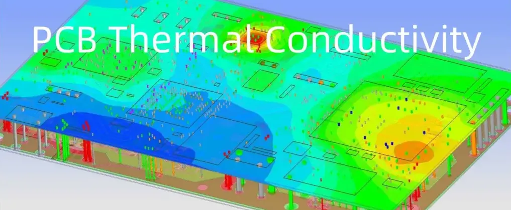
2. Thermal Management Concerns
Since buried vias are enclosed within the PCB, they can contribute to heat buildup in densely packed designs. Without proper thermal vias or heat dissipation strategies, this can affect long-term reliability. Designers can mitigate this by spacing buried vias appropriately and incorporating thermal relief structures where needed.
3. Design and Simulation Requirements
Effective use of buried vias demands precise design and simulation to predict signal behavior. Tools like 3D electromagnetic solvers can model via transitions and identify potential issues with crosstalk or impedance. Investing time in simulation upfront can save costly revisions later, especially for designs operating above 5 GHz.
Best Practices for Implementing Buried Vias in High-Speed PCB Design
To maximize the benefits of buried vias for buried via signal integrity, engineers should follow these practical guidelines during the design process.
- Optimize Layer Stackup: Plan your PCB stackup to place high-speed signals on internal layers connected by buried vias, sandwiching them between ground planes for shielding.
- Control Via Geometry: Use consistent via diameters (e.g., 0.2-0.3 mm) and clearances to maintain impedance and reduce reflections.
- Minimize Via Count: Use only the necessary number of buried vias to avoid cluttering the design and increasing manufacturing complexity.
- Simulate Signal Paths: Leverage simulation software to analyze signal integrity, crosstalk, and impedance before finalizing the layout.
- Collaborate with Manufacturers: Work closely with your PCB fabrication partner to ensure they can support buried via technology within your budget and timeline.
Conclusion: Unlocking the Power of Buried Vias for High-Speed Performance
In the realm of high-speed PCB design, every detail matters. Buried vias offer a hidden advantage by enhancing signal integrity through shorter paths, reduced crosstalk, improved impedance matching, and minimized reflections. While they introduce some manufacturing and design challenges, the benefits for applications like telecommunications, data centers, and advanced computing often outweigh the drawbacks.
By incorporating buried vias strategically and following best practices, engineers can push the boundaries of performance in their designs. Whether you’re working on a 10 Gbps serial link or a 5 GHz RF circuit, leveraging buried vias can be the key to achieving reliable, high-quality signal transmission. As technology continues to evolve, staying ahead of the curve with solutions like buried vias will ensure your designs meet the demands of tomorrow’s innovations.