 ALLPCB


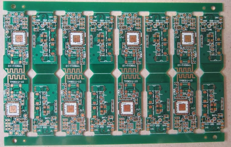
Panelizing PCBs with BGA (Ball Grid Array) components can be a complex process, but with the right practices, you can ensure high-quality assembly, minimize defects, and streamline production. In this comprehensive guide, we’ll dive into the best practices for BGA PCB panelization, covering key areas like minimizing BGA solder bridging, addressing thermal considerations for BGA panels, using x-ray inspection for quality control, and mastering BGA rework techniques on panels. Whether you're an engineer or a manufacturer, this post will provide actionable insights to optimize your panelization process.
Why Panelization Matters for PCBs with BGA Components
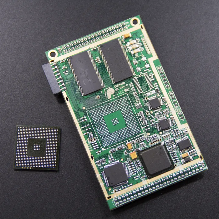
Panelization is the process of grouping multiple PCBs into a single panel for efficient manufacturing and assembly. When dealing with BGA components, which have densely packed solder balls beneath the package, panelization requires extra care. BGA components are widely used in high-performance electronics due to their ability to support high I/O counts (often exceeding 208 leads) in a compact footprint. However, their hidden solder connections make inspection and rework challenging, and improper panelization can lead to issues like solder bridging, thermal stress, or mechanical damage during depanelization.
By following best practices for BGA PCB panelization, you can reduce manufacturing errors, improve yield rates, and ensure the reliability of your final product. Let’s explore the critical aspects of this process in detail.
Key Considerations for BGA PCB Panelization
Successful panelization of PCBs with BGA components starts with careful planning. Below are the foundational steps to ensure your panel design supports both manufacturing efficiency and component integrity.
1. Optimize Panel Layout for BGA Placement
When designing a panel, the placement of BGA components should minimize stress during assembly and depanelization. Keep BGA components away from panel edges or breakaway tabs, as these areas experience high mechanical stress during separation. A clearance of at least 5 mm from the panel edge is recommended to prevent damage to the delicate solder balls, which can be as small as 0.3 mm in diameter for fine-pitch BGAs.
Additionally, ensure uniform spacing between individual PCBs on the panel to avoid uneven heat distribution during reflow soldering. Uneven heating can cause warpage, especially in panels with multiple BGAs, leading to poor solder joint formation.
2. Choose the Right Depanelization Method
Depanelization, the process of separating individual PCBs from the panel, can pose risks to BGA components if not done correctly. Common methods include V-scoring, routing, and breakaway tabs. For BGA panels, routing with pre-milled slots is often preferred because it minimizes mechanical stress compared to V-scoring, which can cause vibrations that damage solder joints. If breakaway tabs are used, ensure they are designed with perforations that require minimal force to separate, reducing the risk of flexing the board near BGA locations.
Minimizing BGA Solder Bridging During Panelization
Solder bridging, where adjacent solder balls connect unintentionally, is a common defect in BGA assembly. During panelization, certain design and process choices can significantly reduce this risk.
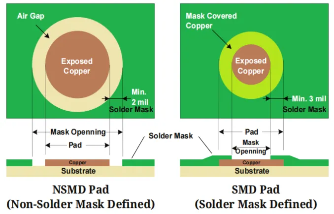
1. Ensure Proper Pad Design and Spacing
The design of solder pads on the PCB plays a critical role in preventing bridging. For BGA components, use non-solder mask defined (NSMD) pads whenever possible. NSMD pads have a larger clearance between the pad and the surrounding solder mask, reducing the chance of solder spreading during reflow. A typical NSMD pad diameter for a 0.5 mm pitch BGA might be 0.25 mm, with a solder mask opening of 0.35 mm to provide adequate spacing.
In panel design, avoid overcrowding PCBs or placing BGAs too close to each other across adjacent boards. This prevents heat buildup in specific areas, which can cause solder to flow uncontrollably and form bridges.
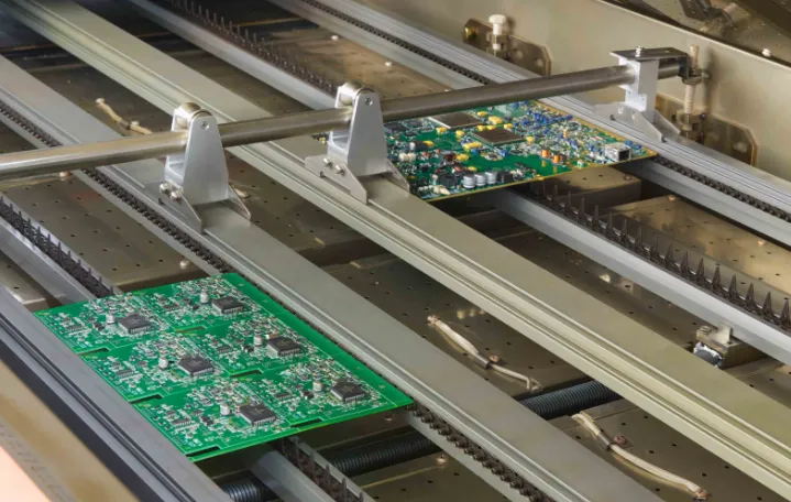
2. Control Reflow Soldering Profiles
During assembly, the reflow soldering profile must be carefully controlled to prevent solder bridging. A gradual ramp-up rate of 1-2°C per second to the peak temperature (typically 240-260°C for lead-free solder) helps ensure even melting of solder balls without excessive flow. Panels with multiple BGAs may require extended soak times (around 60-90 seconds at 150-180°C) to stabilize temperatures across the panel before reaching the reflow zone.
Using nitrogen in the reflow oven can also minimize oxidation on solder balls, reducing the likelihood of defects like bridging. Ensure your manufacturing process accounts for these parameters when handling BGA panels.
Thermal Considerations for BGA Panels
Thermal management is a critical aspect of panelizing PCBs with BGA components. BGAs are sensitive to temperature variations, and poor thermal design can lead to issues like warpage, cold solder joints, or component failure.
1. Balance Copper Distribution
Uneven copper distribution across a panel can cause thermal imbalances during reflow, leading to warpage or uneven solder joint formation. When designing your panel, aim for symmetrical copper coverage by adding dummy copper fills or balancing traces across all PCBs in the panel. For example, if one PCB has a large ground plane under a BGA, replicate similar copper features on other boards in the panel to ensure uniform heat absorption.
2. Use Thermal Relief Pads for Large BGAs
For BGAs with high pin counts (e.g., over 500 pins), thermal relief pads can help manage heat dissipation during soldering. These pads connect to large copper planes with thin spokes, reducing the heat sink effect that can prevent solder balls from melting properly. A typical thermal relief design might use 4 spokes per pad, each 0.2 mm wide, to balance heat flow.
3. Consider Panel Thickness and Material
The choice of PCB material and thickness also impacts thermal performance. For BGA panels, use materials with low coefficients of thermal expansion (CTE), such as FR-4 with a CTE of 14-17 ppm/°C, to minimize mismatch with the BGA package (typically 6-8 ppm/°C). A panel thickness of 1.6 mm is standard for most applications, but for high-density BGAs, consider thinner boards (e.g., 1.0 mm) to reduce thermal mass and improve heat distribution.
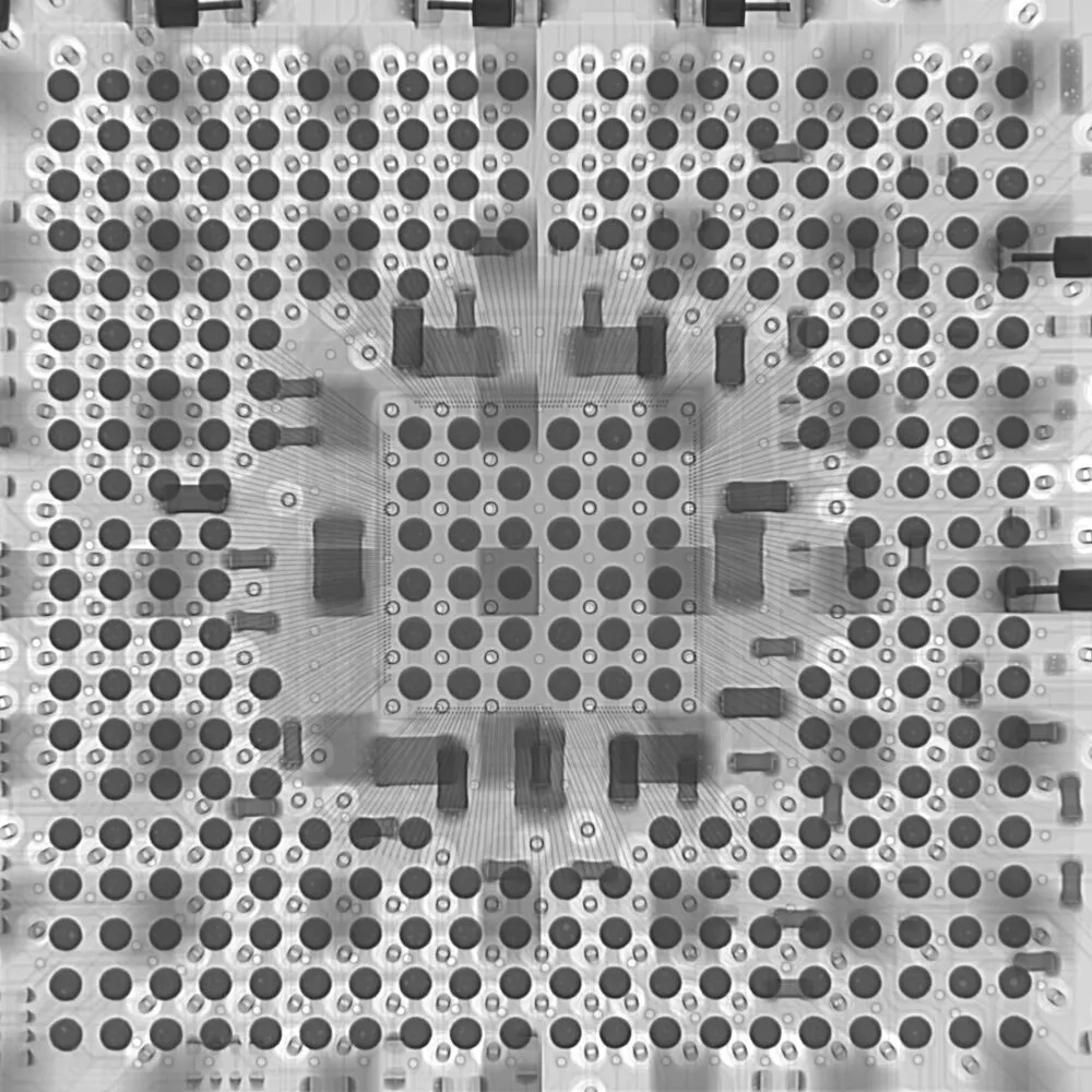
X-Ray Inspection of BGA Panels for Quality Control
Since BGA solder joints are hidden beneath the component, visual inspection is impossible. X-ray inspection is the industry-standard method for evaluating solder joint quality on BGA panels, helping identify defects like voids, bridging, or misalignment.
1. Perform Automated X-Ray Inspection (AXI)
Automated X-ray inspection (AXI) systems can scan entire panels to detect issues with BGA solder joints. These systems analyze the shape and size of solder balls, looking for anomalies such as voids larger than 25% of the solder ball diameter, which can weaken the joint. AXI is particularly useful for high-volume production, as it can inspect multiple BGAs across a panel in a single pass.
2. Focus on Critical Areas
When inspecting BGA panels, pay special attention to solder joints near the panel edges or breakaway tabs, as these areas are prone to defects due to mechanical stress or uneven heating. Adjust the X-ray system to provide higher resolution (e.g., 5-10 μm per pixel) in these critical zones for accurate defect detection.
3. Document and Analyze Defects
After X-ray inspection, maintain detailed records of any defects found, including their location on the panel. This data can help identify patterns, such as recurring issues in specific panel areas, allowing you to adjust your panel design or soldering process. For instance, if voids are consistently found in BGAs near the panel center, it may indicate a thermal imbalance that requires copper redistribution.
BGA Rework Techniques on Panels
Reworking BGA components on a panel can be challenging due to the risk of damaging adjacent PCBs or components. However, with the right tools and techniques, rework can be performed effectively without compromising the panel’s integrity.
1. Use Specialized BGA Rework Stations
BGA rework stations with precise temperature control and hot air nozzles are essential for panel rework. These systems allow you to heat only the target BGA area (typically to 220-240°C for lead-free solder) while protecting surrounding components with thermal shielding. Ensure the rework station has a bottom preheater to maintain uniform panel temperature, preventing warpage during the process.
2. Remove and Replace BGAs Carefully
To remove a defective BGA, apply flux around the component and use the rework station to heat the area until the solder balls melt. Gently lift the BGA with a vacuum tool to avoid damaging the pads. After removal, clean the site with a soldering iron and wick to remove excess solder, then apply fresh solder paste using a mini stencil designed for the specific BGA footprint. Align the replacement BGA using a vision system to ensure precise placement before reflowing.
3. Minimize Thermal Stress on Panels
Reworking a single BGA on a panel can introduce thermal stress to neighboring PCBs. Limit the number of rework cycles to 2-3 per component to avoid degrading the PCB material or nearby solder joints. Additionally, allow the panel to cool gradually after rework (at a rate of 2-3°C per second) to prevent thermal shock.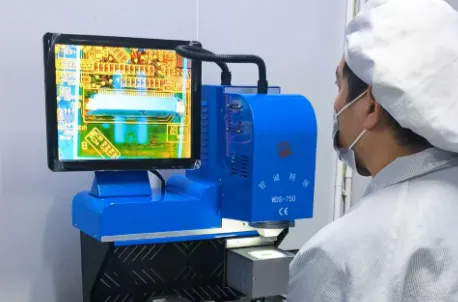
Best Practices for Streamlining BGA Panelization
To wrap up, here are some overarching best practices to ensure success when panelizing PCBs with BGA components:
- Collaborate with Your Manufacturer: Share detailed panel designs and assembly requirements with your manufacturing partner to align on panelization and soldering processes.
- Test Small Batches First: Before full-scale production, assemble and inspect a small batch of panels to identify potential issues with BGA placement or soldering.
- Use Simulation Tools: Leverage thermal and mechanical simulation software to predict panel behavior under reflow conditions, helping you optimize copper distribution and component placement.
- Standardize Processes: Develop and document standardized panelization guidelines for BGA projects to ensure consistency across production runs.
Conclusion
Panelizing PCBs with BGA components requires meticulous attention to design, thermal management, inspection, and rework processes. By following the best practices outlined in this guide—such as optimizing panel layout, minimizing BGA solder bridging, addressing thermal considerations for BGA panels, using x-ray inspection for quality control, and mastering BGA rework techniques on panels—you can achieve reliable, high-quality results. These strategies not only improve manufacturing efficiency but also ensure the long-term performance of your electronic products.
With careful planning and the right tools, BGA PCB panelization can be a seamless part of your production workflow, delivering robust assemblies ready for the most demanding applications.


