 ALLPCB


When designing a printed circuit board (PCB), one of the most critical decisions is selecting the right substrate material. But how do PCB substrate material properties influence spacing requirements? In short, the substrate’s dielectric constant, loss tangent, and thermal properties directly impact trace spacing, signal integrity, and impedance control, especially in high-frequency designs. Choosing the right material ensures optimal performance and prevents issues like signal loss or crosstalk.
In this comprehensive guide, we’ll dive deep into how PCB substrates affect spacing requirements. We’ll explore key material properties like dielectric constant in PCB design, discuss signal loss in PCB materials, and highlight considerations for high-frequency PCB materials. Whether you’re a beginner or an experienced engineer, this PCB material selection guide will help you make informed decisions for your next project.
Understanding PCB Substrates and Their Role in Design
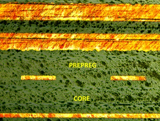
A PCB substrate is the insulating material that sits between the conductive copper layers of a board. It provides mechanical support and electrical insulation while influencing how signals travel through the traces. The properties of the substrate material play a huge role in determining the spacing between traces, especially when dealing with high-speed or high-frequency signals.
Different substrates have unique characteristics, such as dielectric constant (Dk), dissipation factor (Df), and thermal conductivity. These properties affect how closely traces can be placed without risking interference or signal degradation. Let’s break down the key material properties and see how they impact PCB design spacing requirements.
Key PCB Substrate Material Properties and Their Impact
1. Dielectric Constant (Dk) in PCB Design
The dielectric constant, often abbreviated as Dk, measures a material’s ability to store electrical energy in an electric field. It directly affects the speed at which signals propagate through the PCB and the impedance of the traces. Materials with a higher Dk slow down signal transmission, while those with a lower Dk allow faster signal speeds.
For example, FR-4, a commonly used substrate, has a dielectric constant of around 4.2 to 4.5 at 1 MHz. In contrast, high-frequency materials like PTFE-based substrates can have a Dk as low as 2.1. In high-frequency PCB designs, a lower Dk means you can place traces closer together without risking signal interference, as the reduced capacitance between traces minimizes crosstalk.
In practical terms, if you’re working on a design with a 50-ohm impedance requirement, using a material with a Dk of 4.5 might require a trace width of 6 mils and spacing of 8 mils on a standard 1.6mm board. Switch to a material with a Dk of 3.0, and you might reduce spacing to 6 mils while maintaining the same impedance, allowing for a more compact design.
2. Dissipation Factor (Df) and Signal Loss in PCB Materials
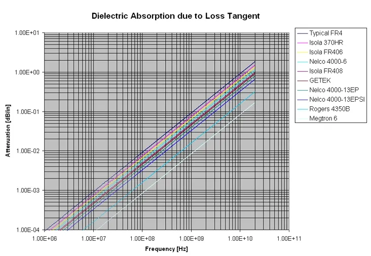
The dissipation factor, or loss tangent, measures how much energy a substrate material loses as heat during signal transmission. A high Df leads to greater signal loss, which is a critical concern in high-frequency PCB materials. For instance, FR-4 has a Df of about 0.02, which is acceptable for low-frequency applications but causes significant signal loss above 1 GHz.
In high-frequency designs, materials with a lower Df, such as Rogers laminates with a Df of 0.001 to 0.003, are preferred. Less signal loss means traces can be spaced closer together without worrying about degradation or noise. If signal loss is high, designers must increase spacing to reduce interference, which can limit how compact the PCB layout can be.
3. Thermal Conductivity and Expansion
Thermal conductivity and the coefficient of thermal expansion (CTE) of a substrate material also influence spacing requirements indirectly. Materials with poor thermal conductivity can lead to hotspots, which may cause traces to expand or contract unevenly. If traces are too close, this can result in shorts or mechanical stress.
For example, FR-4 has a CTE of about 14-17 ppm/°C, while ceramic-based materials can have a CTE as low as 6-8 ppm/°C. In high-power applications, choosing a material with better thermal stability allows for tighter spacing without risking damage due to heat-induced expansion.
How PCB Substrates Affect Spacing in High-Frequency Designs
In high-frequency PCB designs, spacing requirements become even more critical. As frequencies increase, signals are more susceptible to crosstalk, impedance mismatches, and electromagnetic interference (EMI). The choice of substrate material can make or break the performance of such designs.
High-frequency PCB materials, like those with low Dk and Df values, allow for tighter trace spacing while maintaining signal integrity. For instance, at frequencies above 5 GHz, using a material with a Dk of 2.2 can reduce the required spacing between differential pairs by up to 20% compared to standard FR-4. This is because the lower dielectric constant reduces the coupling between adjacent traces, minimizing crosstalk.
Additionally, controlled impedance is vital in high-frequency designs. If the substrate’s Dk varies across the board (due to manufacturing inconsistencies), designers may need to increase spacing to compensate for potential impedance mismatches. Choosing a consistent, high-quality material reduces this risk and allows for a more compact layout.
PCB Material Selection Guide: Choosing the Right Substrate
Selecting the right PCB substrate material is a balancing act between performance, cost, and design requirements. Below is a practical guide to help you choose a material based on your project’s needs, with a focus on how it impacts spacing requirements.
1. Low-Frequency Applications (Below 1 GHz)
For standard digital circuits or low-frequency analog designs, FR-4 is often the go-to choice due to its affordability and availability. With a Dk of around 4.5, it requires moderate spacing to maintain signal integrity. For a 50-ohm impedance, you might need 8-10 mils of spacing between traces, depending on the board thickness and trace width.
2. High-Frequency Applications (1 GHz and Above)
For RF, microwave, or high-speed digital designs, consider materials with lower Dk and Df values. Options like PTFE or specialized laminates allow for tighter spacing, often reducing it to 4-6 mils for the same impedance. These materials are more expensive but essential for minimizing signal loss in PCB materials operating at high frequencies.
3. High-Power or Thermal Applications
In designs with significant heat generation, such as power supplies, prioritize materials with high thermal conductivity and low CTE. Ceramic or metal-core substrates can handle heat better, allowing for closer trace spacing without risking thermal damage. Spacing might still be around 8 mils or more, but the focus is on preventing heat buildup rather than signal integrity.
Practical Tips for Optimizing Spacing with Substrate Choices
Now that we’ve covered the theory behind PCB substrate material properties, let’s look at some actionable tips for optimizing trace spacing in your designs:
- Simulate Before Finalizing: Use PCB design software to simulate signal behavior with different substrate materials. This helps you determine the minimum spacing needed for your target impedance and frequency.
- Match Material to Frequency: Don’t overpay for high-frequency materials if your design operates below 1 GHz. Similarly, avoid using standard materials for RF designs to prevent signal loss.
- Consider Stackup Design: The arrangement of layers and the thickness of the substrate affect impedance and spacing. A thinner substrate often requires wider spacing to maintain the same impedance.
- Account for Manufacturing Tolerances: Some materials have variations in Dk across batches. Add a small buffer to your spacing if you’re working with less consistent materials to avoid surprises.
Common Challenges and Solutions in Material Selection
Even with a solid understanding of PCB substrates, designers often face challenges when balancing spacing requirements with material choices. Here are a few common issues and how to address them:
Challenge 1: Cost Constraints
High-performance materials for high-frequency designs can be expensive. If budget is a concern, consider hybrid stackups where only critical layers use premium materials, while others use cost-effective options like FR-4.
Challenge 2: Signal Loss in PCB Materials
If signal loss is a problem, especially at high frequencies, opt for a material with a lower dissipation factor. Also, increase spacing slightly to reduce crosstalk, even if it means a larger board.
Challenge 3: Thermal Management
For high-power designs, heat dissipation can force wider spacing. Choose a substrate with better thermal conductivity or add thermal vias near critical components to manage heat without sacrificing compactness.
Conclusion: Making Informed Material Choices for Better PCB Designs
The choice of PCB substrate material is a cornerstone of effective PCB design, directly influencing spacing requirements and overall performance. By understanding key properties like dielectric constant in PCB design, signal loss in PCB materials, and the needs of high-frequency PCB materials, you can optimize trace spacing for signal integrity and compactness.
Whether you’re designing a simple low-frequency board or a complex RF circuit, this PCB material selection guide provides the foundation to make informed decisions. Remember to match the substrate to your application’s frequency, thermal, and budget needs. With the right material, you can achieve tighter spacing, reduce signal loss, and ensure reliable performance in any project.


