 ALLPCB


In today’s educational landscape, creating inclusive learning environments is more important than ever. For students learning electronics, particularly those with disabilities, accessible PCB (Printed Circuit Board) design can make a significant difference. How can educators and designers ensure that PCB projects are usable by everyone, including visually impaired students or those with motor skill challenges? The answer lies in thoughtful, inclusive design practices that prioritize accessibility from the start.
This blog post explores the best practices for designing educational electronics PCBs with accessibility in mind. We’ll cover strategies for creating universally designed PCB learning kits, tips for accommodating students with diverse needs, and actionable steps to foster inclusive electronics education. Whether you’re an educator, designer, or student, these insights will help you build projects that empower all learners. Let’s dive into the world of accessible electronics project design.
Why Accessibility Matters in Electronics Education
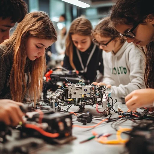
Electronics education often involves hands-on activities like designing and assembling PCBs. These tasks can be challenging for students with disabilities if the tools, materials, and designs are not accessible. For instance, visually impaired students may struggle with small components or unreadable schematics, while students with motor skill challenges might find soldering tiny parts nearly impossible. Without inclusive design, these students risk being excluded from valuable learning experiences.
By focusing on accessible PCB design for visually impaired students and designing PCBs for students with motor skill challenges, we can create learning environments where everyone has the opportunity to succeed. Inclusive electronics education not only benefits students with disabilities but also encourages creativity and problem-solving among all learners. Let’s explore how to make this a reality with practical design strategies.
Key Principles of Accessible PCB Design
Creating accessible electronics project designs starts with understanding the core principles of inclusivity. These principles guide the development of universally designed PCB learning kits that cater to a wide range of abilities. Here are the foundational ideas to keep in mind:
- Simplicity: Keep designs straightforward to reduce complexity for all users. Avoid overcrowded layouts with too many components or tight spacing.
- Flexibility: Offer multiple ways to interact with the PCB, such as larger components for easier handling or digital simulations for those who can’t physically assemble boards.
- Perceptibility: Ensure that information is conveyed in multiple formats, like tactile markers or audio feedback, to support students with visual or auditory impairments.
- Tolerance for Error: Design PCBs that are forgiving, with clear labeling and reversible assembly steps to minimize frustration.
By applying these principles, designers can create educational tools that work for everyone. Now, let’s break down specific strategies for addressing common accessibility challenges in PCB design.
Designing PCBs for Visually Impaired Students
Accessible PCB design for visually impaired students requires careful attention to how information is presented and how components are arranged. Here are some best practices to consider:
1. Use Tactile Features
Incorporate tactile elements into the PCB layout, such as raised markings or textured surfaces, to help students identify components and connections by touch. For example, use different textures to distinguish between power and ground lines. This allows students to “feel” the board’s layout without relying solely on sight.
2. Provide High-Contrast Visuals
For students with partial vision, high-contrast colors on the PCB and accompanying schematics can improve readability. Use bold, large fonts for labels and ensure that traces and components stand out against the board’s background. A contrast ratio of at least 4.5:1 between text and background is recommended for readability.
3. Include Audio or Digital Support
Pair physical PCBs with digital tools that offer audio descriptions of the board layout or components. Software simulations can also read out connection details or provide step-by-step guidance, ensuring visually impaired students can follow along with their peers.
Designing PCBs for Students with Motor Skill Challenges
Students with motor skill challenges, such as limited hand dexterity or tremors, face unique obstacles when working with traditional PCBs. Designing PCBs for students with motor skill challenges involves making physical interaction easier and less precise. Here are some effective approaches:
1. Opt for Larger Components and Spacing
Use larger components, such as through-hole parts instead of surface-mount devices (SMDs), which are easier to handle and solder. Increase the spacing between components to at least 2.54 mm (0.1 inches) to prevent accidental short circuits and make assembly less demanding on fine motor control.
2. Simplify Assembly Processes
Reduce the number of steps required to assemble the PCB. Pre-solder certain components or use snap-together connectors instead of soldering wherever possible. This minimizes the need for precise movements and reduces physical strain.
3. Provide Supportive Tools
Include adaptive tools in learning kits, such as magnetic component holders or soldering aids with grips. These tools can stabilize hands and make tasks like placing components or soldering more manageable for students with motor challenges.
Creating Universally Designed PCB Learning Kits
Universally designed PCB learning kits are essential for inclusive electronics education. These kits should cater to a variety of needs while maintaining educational value. Here’s how to build kits that work for all students:
1. Modular Design
Create kits with modular components that can be easily swapped or adjusted. For example, offer boards with pre-drilled holes for different component sizes or layouts that can be customized based on a student’s ability level. This flexibility ensures that no one is left out due to a one-size-fits-all approach.
2. Comprehensive Documentation
Provide instructions in multiple formats, including text, audio, and video. Ensure that written guides use large, clear fonts and simple language. Include diagrams with high-contrast colors and tactile versions for visually impaired students. Documentation should also cover alternative assembly methods for those with physical limitations.
3. Scalable Difficulty
Design kits with projects of varying difficulty levels. Start with basic circuits that require minimal assembly and progress to more complex designs. This allows students to build skills at their own pace, regardless of their starting point or physical abilities.
Best Practices for Inclusive Electronics Education
Beyond the physical design of PCBs and kits, fostering inclusive electronics education requires a supportive learning environment. Here are some best practices for educators and institutions:
1. Train Educators on Accessibility
Equip teachers with the knowledge and tools to support students with disabilities. Training should cover how to use accessible materials, adapt lessons for different needs, and create an inclusive classroom culture. Understanding the challenges students face is the first step to addressing them effectively.
2. Encourage Collaboration
Promote teamwork among students of varying abilities. Pairing students for projects allows them to learn from each other’s strengths. For example, a visually impaired student might excel at conceptual design, while a peer with strong motor skills handles assembly. Collaboration builds confidence and fosters a sense of community.
3. Leverage Technology
Use technology to bridge accessibility gaps. Digital simulations of PCB designs can help students visualize circuits without needing to assemble them physically. Assistive devices, like voice-activated software or magnifying tools, can also enhance participation for students with specific needs.
Technical Considerations for Accessible PCB Design
When designing accessible PCBs, certain technical aspects can improve usability. While keeping the language simple, let’s look at a few specifics that can make a big difference:
- Trace Width and Spacing: Use wider traces (at least 0.25 mm or 10 mils) and spacing to make soldering easier and reduce the risk of errors. This is especially helpful for students with motor skill challenges who may struggle with precision.
- Power Distribution: Design boards with clear power and ground planes to minimize confusion. Label these areas with tactile or high-contrast markers for better identification.
- Component Placement: Group related components together logically and label them clearly. For example, place resistors near the circuits they support and mark their values in large, readable text or Braille.
These small adjustments in design can significantly improve the user experience for students with diverse needs, ensuring that technical barriers don’t stand in the way of learning.
Challenges and Solutions in Accessible Electronics Project Design
While designing accessible electronics projects is rewarding, it comes with challenges. Here are a few common hurdles and how to overcome them:
1. Cost of Accessibility Features
Adding tactile elements, larger components, or adaptive tools can increase production costs. To manage this, focus on scalable designs that use cost-effective materials. For instance, 3D-printed tactile markers can be an affordable way to add texture to PCBs.
2. Balancing Simplicity and Learning Value
Simplifying designs for accessibility might reduce the complexity of projects, potentially limiting advanced learning. Address this by offering optional challenges or digital simulations that allow students to explore more complex concepts without physical barriers.
3. Time Constraints in Education
Creating accessible materials and training educators takes time, which can be limited in academic settings. Start with small, incremental changes, such as updating one project or kit at a time, and build toward broader inclusivity over time.
Conclusion: Building an Inclusive Future in Electronics Education
Designing educational electronics PCBs for accessibility is not just about meeting technical requirements—it’s about empowering every student to participate in the exciting world of electronics. By focusing on accessible PCB design for visually impaired students, designing PCBs for students with motor skill challenges, and creating universally designed PCB learning kits, we can ensure that inclusive electronics education becomes the standard.
Start small by incorporating tactile features, using larger components, and providing comprehensive instructions in multiple formats. Over time, these efforts will build a more inclusive learning environment where all students can thrive. At ALLPCB, we’re committed to supporting educators and designers in this mission, offering resources and expertise to bring accessible electronics project design to life.
By embracing these best practices, we can shape a future where no student is left behind in their journey to master electronics. Let’s work together to make education truly inclusive for everyone.


