 ALLPCB


If you're designing complex electronics, especially for high-speed applications, a 12-layer PCB stackup is often the go-to solution for balancing signal integrity, power distribution, and impedance control. But what exactly is a 12-layer PCB stackup, and how can you design one to meet the demands of high-speed circuits? In this guide, we'll break down the essentials of 12-layer PCB stackup design, covering impedance control, signal integrity, materials, design rules, and cost considerations. Whether you're an engineer or a designer, you'll find actionable insights to optimize your next project.
Let’s dive into the details of designing a 12-layer PCB stackup for high-speed designs. From understanding its structure to mastering the best practices, this comprehensive guide will help you navigate the complexities and achieve top-notch performance.
What Is a 12-Layer PCB Stackup and Why Use It for High-Speed Designs?
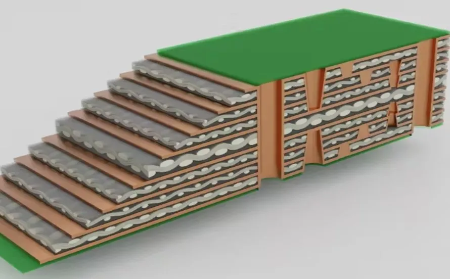
A 12-layer PCB stackup refers to the arrangement of conductive copper layers and insulating dielectric layers in a printed circuit board with 12 total layers. These layers are carefully organized to handle various functions, such as signal routing, power distribution, and grounding, especially in high-speed and high-frequency applications like telecommunications, data centers, and advanced computing systems.
High-speed designs often involve signals operating at frequencies above 100 MHz, where issues like crosstalk, electromagnetic interference (EMI), and signal loss become significant challenges. A 12-layer stackup provides enough layers to separate high-speed signals, dedicate planes for power and ground, and control impedance effectively. This structure helps minimize noise and ensures reliable performance, making it ideal for complex circuits.
Key Benefits of a 12-Layer PCB Stackup
- Enhanced Signal Integrity: Multiple layers allow for dedicated signal routing and shielding, reducing interference.
- Improved Power Distribution: Separate power and ground planes ensure stable voltage delivery.
- Impedance Control: Precise layer arrangement helps maintain consistent impedance for high-speed signals.
- Compact Design: More layers mean denser circuitry in a smaller footprint, critical for modern devices.
Understanding 12-Layer PCB Stackup Impedance Control
Impedance control is a cornerstone of high-speed PCB design. In a 12-layer PCB stackup, impedance refers to the resistance a signal encounters as it travels through a trace, influenced by the trace width, dielectric thickness, and material properties. Mismatched impedance can lead to signal reflections, data errors, and performance degradation.
To achieve proper 12-layer PCB stackup impedance control, designers must carefully plan the layer arrangement and material selection. For example, high-speed signals often require a characteristic impedance of 50 ohms for single-ended traces or 100 ohms for differential pairs. Here's how to approach it:
- Layer Symmetry: Arrange signal layers symmetrically around the center of the stackup to balance stresses and maintain consistent impedance.
- Reference Planes: Place high-speed signal layers adjacent to continuous ground or power planes to provide a stable reference for impedance.
- Trace Geometry: Use impedance calculators to determine the correct trace width and spacing based on the dielectric constant (Dk) of the material, often around 3.5 to 4.5 for standard FR-4.
For instance, if you're routing a 50-ohm trace on layer 2, ensure it's referenced to a ground plane on layer 3 with a dielectric thickness of about 0.1 mm to achieve the desired impedance. Tools like field solvers or PCB design software can help simulate and verify these values before fabrication.
Optimizing 12-Layer PCB Stackup for Signal Integrity
Signal integrity (SI) is the ability of a signal to maintain its shape and timing as it travels through the PCB. Poor SI can result in data corruption, timing errors, and system failures. A well-designed 12-layer PCB stackup for signal integrity addresses these issues by minimizing noise and interference.
Best Practices for Signal Integrity in a 12-Layer Stackup
- Dedicated Signal Layers: Use inner layers (e.g., layers 2, 4, 9, 11) for high-speed signals to shield them from external noise.
- Ground Plane Proximity: Keep high-speed signals close to a ground plane to reduce loop inductance and EMI.
- Minimize Crosstalk: Route critical signals on separate layers or maintain adequate spacing (e.g., 3x the trace width) to avoid interference.
- Via Management: Use back-drilling or blind vias to reduce stub effects that degrade signal quality at frequencies above 1 GHz.
For example, in a 12-layer stackup, you might allocate layers 1 and 12 for low-speed signals or components, layers 2 and 11 for high-speed signals, and layers 3, 5, 8, and 10 as ground planes to sandwich the signals and provide shielding. This setup helps maintain clean signal paths and reduces EMI risks.
Choosing the Right 12-Layer PCB Stackup Materials
The materials used in a PCB directly impact its performance, especially for high-speed designs. When selecting 12-layer PCB stackup materials, you need to consider factors like dielectric constant (Dk), loss tangent (Df), thermal stability, and cost.
Common Materials for 12-Layer Stackups
- FR-4: A cost-effective standard material with a Dk of around 4.2–4.5, suitable for frequencies up to 1 GHz. However, it has higher signal loss at higher frequencies.
- High-Speed Laminates: Materials like Isola 370HR or Rogers 4350B offer lower Dk (around 3.0–3.5) and lower loss tangent (0.003–0.009), ideal for frequencies above 1 GHz.
- Prepreg and Core: Use compatible prepreg (resin layers) and core materials to ensure uniform dielectric properties across the stackup.
For high-speed designs, using a hybrid stackup—combining FR-4 for power and ground layers with high-speed laminates for signal layers—can balance performance and cost. Additionally, ensure the material's thermal expansion coefficient (CTE) matches to prevent warping during manufacturing or operation.
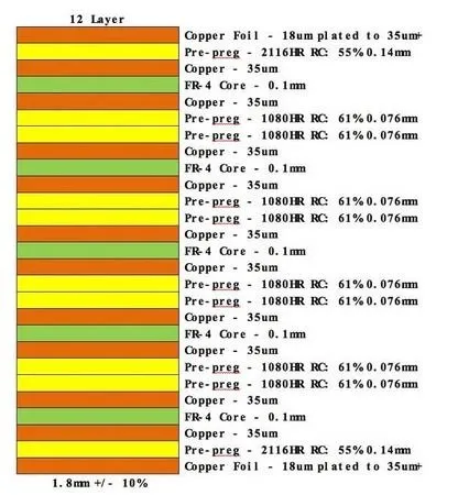
Essential 12-Layer PCB Stackup Design Rules
Following strict 12-layer PCB stackup design rules is critical to avoid manufacturing issues and ensure the board performs as intended. These rules cover layer arrangement, spacing, and routing practices tailored for high-speed applications.
Key Design Rules to Follow
- Symmetrical Stackup: Maintain symmetry in layer thickness and material to prevent board warpage. For example, if layer 1 is a signal layer, layer 12 should mirror it.
- Power and Ground Planes: Dedicate at least two layers each for power and ground to ensure low impedance paths and effective decoupling. Place them centrally (e.g., layers 6 and 7) for balance.
- Dielectric Thickness: Keep dielectric spacing consistent between signal and reference layers (e.g., 0.1–0.2 mm) to maintain impedance.
- Routing Guidelines: Avoid routing high-speed signals across split planes, as this disrupts the return path and causes EMI.
- Via Placement: Minimize via transitions for high-speed signals and use ground vias nearby to provide a return path.
By adhering to these rules, you can reduce manufacturing defects and ensure the stackup supports the high-speed requirements of your design. Always consult with your fabrication partner early in the design process to confirm their capabilities and constraints.
Analyzing 12-Layer PCB Stackup Cost Factors
Cost is a significant concern when designing a 12-layer PCB stackup. While more layers offer better performance, they also increase production complexity and expenses. Understanding the factors that drive 12-layer PCB stackup cost can help you make informed decisions without compromising quality.
Factors Influencing Cost
- Material Selection: High-speed laminates cost more than standard FR-4. For instance, using advanced materials only for critical signal layers can save money.
- Layer Count: A 12-layer board is inherently more expensive than a 4- or 6-layer board due to additional processing steps.
- Manufacturing Complexity: Features like blind vias, tight tolerances, or thin dielectrics increase fabrication costs.
- Volume: Higher production volumes often reduce per-unit costs, while small batches are pricier due to setup fees.
- Testing Requirements: Impedance testing or advanced quality checks add to the overall expense but ensure reliability.
To optimize costs, consider using standard materials where high-speed performance isn’t critical and simplify the design by reducing via types or layer transitions. Working closely with your manufacturing partner can also uncover cost-saving opportunities without sacrificing performance.
Practical Tips for Designing a 12-Layer PCB Stackup
Designing a 12-layer PCB stackup for high-speed applications can be daunting, but these practical tips can streamline the process and improve outcomes:
- Start with Simulation: Use PCB design software to simulate impedance, signal integrity, and EMI before finalizing the stackup.
- Collaborate Early: Engage with your fabrication team during the design phase to align on material availability and manufacturing limits.
- Prioritize Critical Signals: Allocate the best-shielded layers to the fastest signals, reserving outer layers for less sensitive traces.
- Document Everything: Maintain detailed notes on layer functions, impedance targets, and material specs for future reference or troubleshooting.
By following these steps, you can avoid common pitfalls and create a stackup that meets both technical and budgetary goals.
Conclusion: Mastering 12-Layer PCB Stackups for High-Speed Success
Designing a 12-layer PCB stackup for high-speed applications is a balancing act between performance, complexity, and cost. By focusing on 12-layer PCB stackup impedance control, ensuring signal integrity, selecting the right materials, adhering to design rules, and managing cost, you can create a robust and reliable board for even the most demanding projects.
This guide has walked you through the critical aspects of 12-layer stackup design, from understanding its structure to applying best practices. Armed with this knowledge, you're better equipped to tackle the challenges of high-speed PCB design and deliver cutting-edge solutions. Keep iterating, testing, and refining your approach to stay ahead in the fast-paced world of electronics design.


