 ALLPCB


The world of electronics is evolving rapidly, and at the heart of this transformation is the printed circuit board (PCB). Prototyping these critical components has traditionally been a time-consuming and costly process, but 3D-printed electronics are changing the game. By enabling faster, more flexible, and sustainable prototyping, this technology is poised to redefine how engineers design and test PCBs. In this blog, we explore the potential of 3D-printed electronics, their advantages, challenges, and what they mean for the future of PCB prototyping.
Whether you're an engineer looking to streamline your workflow or a company aiming to stay ahead of industry trends, understanding 3D-printed electronics is essential. Let's dive into how this innovative approach is shaping the future.
What Are 3D-Printed Electronics?
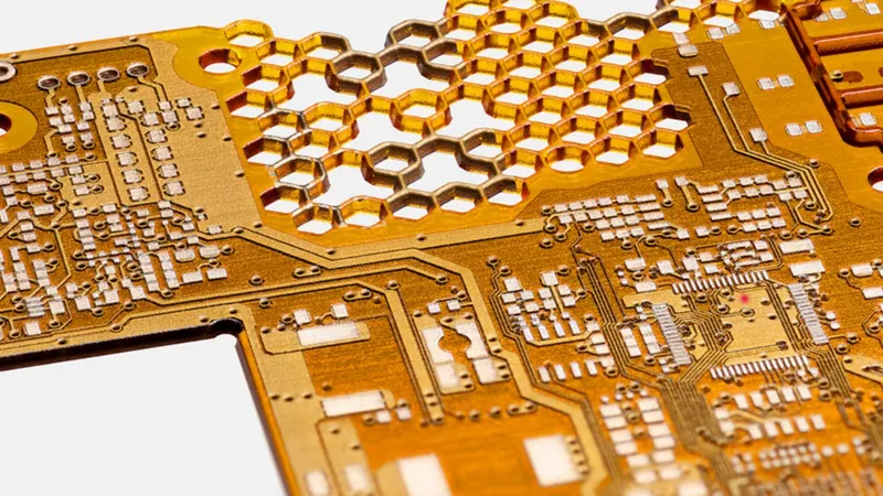
3D-printed electronics involve using additive manufacturing to create functional electronic components, including PCBs, by depositing conductive and dielectric materials layer by layer. Unlike traditional PCB prototyping, which relies on subtractive methods like copper etching, 3D printing builds circuits directly from digital designs. This process allows for the creation of complex, multi-layered boards with intricate geometries that would be challenging or impossible to achieve with conventional techniques.
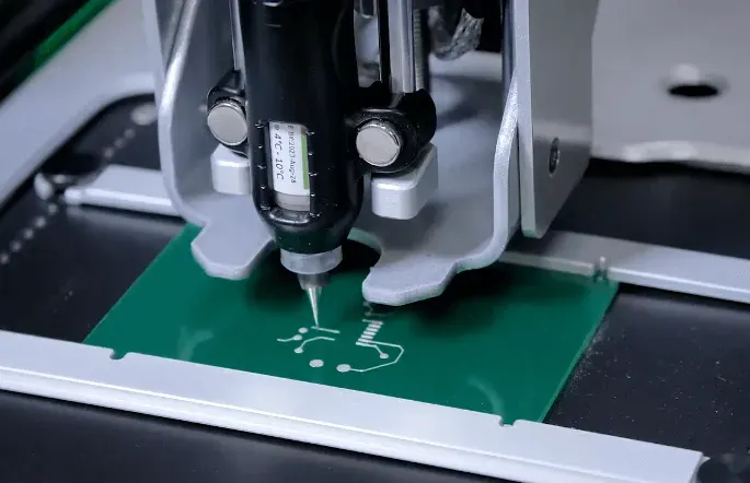
The technology typically uses specialized 3D printers, such as Nano Dimension's DragonFly IV, which can print conductive inks (often silver or copper-based) and dielectric polymers simultaneously. These printers can produce boards with trace widths as small as 80 micrometers and layer thicknesses down to 30 micrometers, offering precision comparable to traditional methods. The result is a fully functional PCB prototype that can be tested for performance, signal integrity, and impedance control.
Why 3D Printing for PCB Prototyping?
The shift toward 3D-printed electronics is driven by several compelling advantages that address the pain points of traditional PCB prototyping. Here are the key benefits:
Speed and Rapid Iteration
Traditional PCB prototyping can take weeks, involving multiple steps like design, fabrication, and assembly. In contrast, 3D printing can produce a functional prototype in as little as 24 hours. For example, companies like Lprint claim their 3D printing systems can cut production time by eliminating the need for outsourcing and reducing iteration cycles. This speed is critical for engineers working on tight deadlines or iterating designs for high-speed applications, where signal integrity and impedance (typically 50 ohms for single-ended traces) must be validated quickly.
Design Flexibility
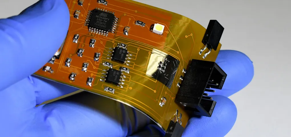
3D printing enables the creation of non-planar and flexible PCBs, which are ideal for compact devices like wearables or IoT sensors. Unlike rigid boards, 3D-printed circuits can conform to curved surfaces or fit into irregular shapes, supporting innovative product designs. For instance, a 3D-printed antenna system operating at 19 GHz has been demonstrated, showcasing the technology's ability to handle high-frequency applications with precise control over dielectric properties.
Cost-Effectiveness for Prototyping
While traditional prototyping requires expensive tooling and minimum order quantities, 3D printing eliminates these barriers. The additive process minimizes material waste, as only the necessary conductive and dielectric materials are used. For small-batch or single-unit prototypes, this can reduce costs by up to 50% compared to subtractive methods, especially for complex designs with high-density interconnects (HDI).
Sustainability
Traditional PCB manufacturing generates significant chemical waste, with etching processes producing an estimated 1 trillion liters of toxic byproducts annually. 3D printing, by contrast, is more environmentally friendly, using biodegradable materials and consuming less energy. This aligns with the growing demand for sustainable electronics, particularly in industries like medical devices and consumer electronics.
Challenges of 3D-Printed Electronics
Despite its promise, 3D-printed electronics face several hurdles that must be addressed before they can fully replace traditional methods. Understanding these challenges helps engineers make informed decisions about when to adopt this technology.
Material Limitations
Current 3D printing materials, such as copper-doped polymers, cannot yet match the performance of silicon-based semiconductors. For example, MIT researchers have developed 3D-printed logic gates that function as resettable fuses but operate at lower speeds than traditional transistors. These materials are suitable for basic control tasks, like regulating a motor's speed, but struggle with high-performance applications requiring nanometer-scale transistors.
Scalability
While 3D printing excels in prototyping, it is not yet viable for mass production. The layer-by-layer printing process is slower than automated assembly lines, and the cost of conductive inks remains high. For high-volume manufacturing, traditional methods still offer better economies of scale, producing boards with consistent impedance (e.g., 100 ohms for differential pairs) at lower costs.
Software Integration
Designing 3D-printed electronics requires specialized software to handle complex geometries and material properties. Most electronic computer-aided design (ECAD) tools, like Altium or Cadence, are optimized for 2D layouts, making it difficult to route traces in 3D space. While some platforms, like Lprint's software, convert Gerber files into 3D models for printing, the lack of standardized tools limits widespread adoption.
Applications Driving Adoption
The versatility of 3D-printed electronics is unlocking new possibilities across various industries. Here are some key applications where this technology is making an impact:
Aerospace and Defense
In aerospace, 3D-printed electronics enable lightweight, conformal circuits for satellites and drones. For example, Nano Dimension's technology has been used to prototype RF amplifiers and antennas, reducing weight by 20% compared to traditional boards while maintaining signal integrity at frequencies up to 5 GHz.
Medical Devices
Flexible 3D-printed PCBs are ideal for wearable medical devices, such as pacemakers and glucose monitors, where space and comfort are critical. These boards can be printed with biocompatible materials, ensuring safety and reliability in high-stakes applications.
Consumer Electronics
The demand for smaller, more powerful devices like smartphones and smartwatches is driving the adoption of 3D-printed HDI boards. These boards support fine-pitch components with pin-to-pin spacing as low as 0.6 mm, enabling compact designs without compromising performance.
How ALLPCB Supports the Future of Prototyping
At ALLPCB, we understand the importance of staying at the forefront of PCB prototyping technologies. While 3D-printed electronics are transforming the industry, traditional prototyping remains essential for many applications. Our quick-turn prototyping services, with turnaround times as fast as 24 hours, complement the speed of 3D printing, ensuring engineers can test and iterate designs efficiently. With global logistics and advanced manufacturing capabilities, we provide high-quality PCBs that meet stringent standards, such as IPC Class 2 and 3, supporting industries from aerospace to consumer electronics.
The Future of PCB Prototyping
3D-printed electronics are not just a trend; they represent a paradigm shift in PCB prototyping. By offering unmatched speed, flexibility, and sustainability, this technology empowers engineers to push the boundaries of design. However, challenges like material limitations and scalability mean that traditional methods will coexist with 3D printing for the foreseeable future. As materials improve and software tools evolve, we expect 3D-printed electronics to play a larger role in both prototyping and low-volume production.
For engineers, the key is to leverage the strengths of both approaches. Use 3D printing for rapid iteration and complex geometries, and rely on traditional prototyping for high-volume or performance-critical applications. By staying informed about these advancements, you can make strategic decisions that accelerate your projects and reduce costs.
Conclusion
The rise of 3D-printed electronics marks an exciting chapter in PCB prototyping. With the ability to create complex, functional prototypes in hours rather than weeks, this technology is empowering engineers to innovate faster and more efficiently. While challenges remain, the potential for 3D printing to transform industries like aerospace, medical, and consumer electronics is undeniable. At ALLPCB, we're committed to supporting this evolution by providing cutting-edge prototyping solutions that meet the needs of today's engineers. As we look to the future, 3D-printed electronics may well be the key to unlocking the next generation of electronic devices.


