ALLPCB


In the world of printed circuit board (PCB) design, precision is everything. One critical aspect that often gets overlooked is via-to-via spacing. So, what are the IPC standards for via-to-via spacing? The IPC-2221 standard, a key guideline for PCB design, does not explicitly define a fixed via-to-via spacing value. Instead, it provides recommendations based on electrical clearance, manufacturing constraints, and design requirements like voltage levels and signal integrity. Factors such as the PCB class (Class 1, 2, or 3) and the operating environment also play a role in determining appropriate spacing.
In this blog post, we’ll dive deep into via-to-via spacing under IPC standards, explore how these guidelines ensure reliable and high-performing PCB designs, and provide actionable insights for engineers and designers. Whether you’re working on a simple prototype or a complex multilayer board, understanding these standards is essential for success.
What Are IPC Standards and Why Do They Matter in PCB Design?
IPC standards are a set of guidelines developed by the Institute of Printed Circuits (now known as IPC - Association Connecting Electronics Industries). These standards aim to ensure quality, reliability, and consistency in the design, manufacturing, and assembly of electronic products, including PCBs. They cover everything from material selection to component placement, trace widths, and via designs.
For PCB designers, adhering to IPC standards is crucial. They provide a universal framework that helps avoid common design flaws, ensures manufacturability, and meets safety requirements. When it comes to via-to-via spacing, following IPC guidelines prevents issues like electrical shorts, signal interference, and mechanical failures during production.
Key IPC Standards Relevant to Vias and Spacing
While there are many IPC standards, a few are particularly relevant to via-to-via spacing:
- IPC-2221: This is the generic standard for PCB design. It provides guidance on spacing for electrical clearance and creepage distances based on voltage levels and environmental conditions.
- IPC-6012: Focuses on the qualification and performance of rigid PCBs, including via structures and manufacturing tolerances.
- IPC-A-610: Covers acceptability criteria for electronic assemblies, often referencing via placement and spacing for quality control.
These standards collectively ensure that your PCB design can handle the intended electrical load, withstand environmental stresses, and be manufactured without defects.
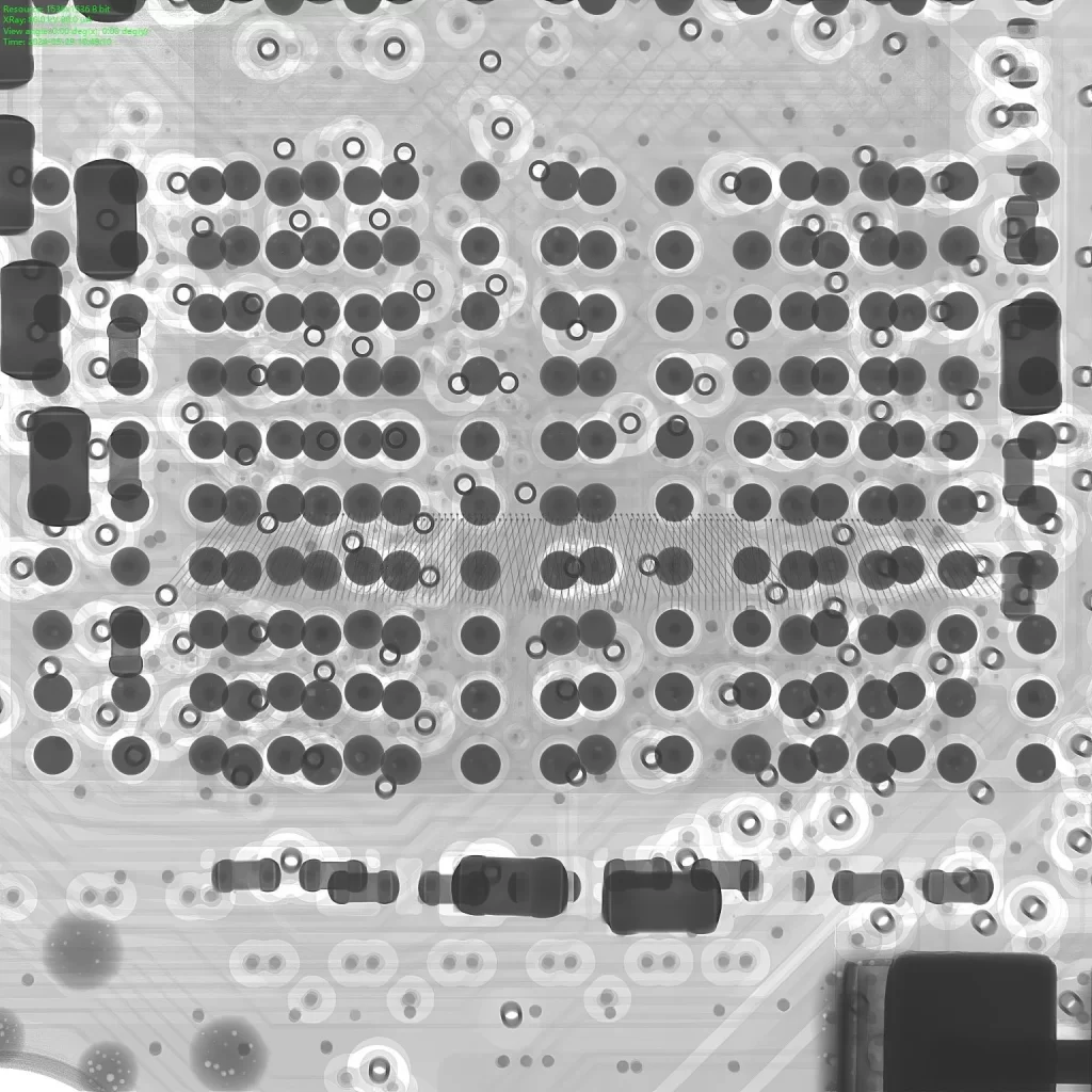
Understanding Via-to-Via Spacing in PCB Design
Vias are small holes in a PCB that allow electrical connections between different layers of the board. They are essential for multilayer designs, enabling signals and power to travel through the board. However, placing vias too close to each other can lead to several problems, including:
- Electrical Interference: Close vias can cause crosstalk or electromagnetic interference (EMI), degrading signal integrity.
- Manufacturing Issues: Insufficient spacing may lead to drilling errors or structural weaknesses in the PCB.
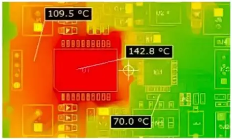
- Thermal Stress: Vias that are too close can create heat buildup, risking damage during soldering or operation.
Via-to-via spacing refers to the minimum distance between the centers or edges of two adjacent vias. This spacing must be carefully calculated to avoid these issues while meeting the design’s functional and manufacturing requirements.
Factors Influencing Via-to-Via Spacing
IPC standards don’t provide a one-size-fits-all number for via-to-via spacing. Instead, they encourage designers to consider several factors:
- Voltage Levels: Higher voltages require greater spacing to prevent arcing or electrical breakdown. For example, IPC-2221 suggests a minimum clearance of 0.6 mm for voltages up to 100V under certain conditions.
- PCB Class: IPC defines three classes of PCBs—Class 1 (general electronics), Class 2 (dedicated service electronics), and Class 3 (high-reliability electronics). Class 3 designs, used in aerospace or medical devices, demand stricter spacing for reliability.
- Signal Type: High-speed signals, such as those operating at 5 GHz, are more prone to interference, requiring wider spacing to maintain signal integrity.
- Manufacturing Capabilities: The precision of the drilling and plating processes affects how close vias can be placed. Typical minimum via-to-via spacing for standard manufacturing might be around 0.3 mm center-to-center, but this varies by fabricator.
- Environmental Conditions: Harsh environments with high humidity or pollution may necessitate larger spacing to prevent creepage (current leakage across the surface).
By balancing these factors, designers can determine the optimal via-to-via spacing for their specific project.
Related Reading: Via to Via Spacing for Beginners: A Friendly Guide
IPC Guidelines for Via-to-Via Spacing
As mentioned earlier, IPC-2221 is the primary standard for PCB design and provides the foundation for via spacing. While it doesn’t specify exact via-to-via spacing, it offers tables and formulas for electrical clearance and creepage distances. These can be adapted to determine safe spacing between vias based on the design’s voltage and environmental factors.
Electrical Clearance and Creepage Distances
IPC-2221 defines clearance as the shortest distance through air between conductive elements, while creepage is the shortest distance along the surface of the insulating material. For vias, both concepts are critical to prevent unintended electrical connections.
- For voltages up to 100V, a typical clearance distance might be 0.6 mm, though this increases with higher voltages.
- Creepage distances are often larger, especially in polluted or humid environments, and can range from 0.8 mm to several millimeters depending on conditions.
Designers must ensure that via-to-via spacing meets or exceeds these clearance and creepage values to avoid electrical failures.
Via Annular Ring and Pad Size Considerations
The annular ring (the copper ring around a via) and pad size also influence spacing. IPC-6012 specifies minimum annular ring sizes to ensure structural integrity during drilling and plating. For example, a minimum annular ring of 0.05 mm might be required for Class 2 boards. If the annular ring or pad is larger, the via-to-via spacing must increase accordingly to maintain clearance between conductive elements.
High-Speed Design Considerations
In high-speed PCB designs, via-to-via spacing becomes even more critical due to signal integrity concerns. Vias can act as stubs or introduce impedance mismatches if not spaced properly. For signals operating at 10 GHz, for instance, spacing vias at least 1.5 times the via diameter (e.g., 0.45 mm for a 0.3 mm via) can help reduce crosstalk. While IPC standards don’t directly address high-speed design spacing, they encourage designers to consider signal performance alongside basic clearance rules.
Practical Tips for Implementing Via-to-Via Spacing in Your Designs
Now that we’ve covered the theory behind IPC standards for via-to-via spacing, let’s look at some practical steps to apply these guidelines in your PCB projects.
1. Use Design Software with IPC Compliance Tools
Modern PCB design software often includes built-in design rule checks (DRC) aligned with IPC standards. Set up rules for minimum via-to-via spacing based on your project’s voltage, class, and signal requirements. For instance, if you’re designing a Class 3 board for 200V operation, input a clearance of at least 1.5 mm as a starting point, then adjust based on other factors.
2. Collaborate with Your Manufacturer
Every PCB manufacturer has specific capabilities and limitations when it comes to via drilling and spacing. Early collaboration can help you align your design with their process, avoiding costly redesigns. For example, if their minimum drill-to-drill spacing is 0.4 mm, ensure your via-to-via spacing accommodates this limit.
3. Test and Validate Your Design
Before finalizing your design, run simulations to check for signal integrity issues, especially in high-speed applications. Tools like SPICE or electromagnetic simulators can help identify potential crosstalk or EMI caused by closely spaced vias. Adjust spacing as needed to meet performance goals.
4. Consider Multilayer Design Strategies
In multilayer boards, vias often pass through multiple layers, increasing the risk of interference. Staggering vias (placing them in non-adjacent positions on different layers) can help maintain spacing and reduce signal coupling. IPC standards encourage such strategies for complex designs.
Related Reading: How Via to Via Spacing affects the power plane?
Common Mistakes to Avoid with Via-to-Via Spacing
Even experienced designers can make errors when it comes to via spacing. Here are some pitfalls to watch out for:
- Ignoring Voltage Ratings: Failing to account for the operating voltage can lead to insufficient clearance, risking arcing or shorts.
- Overlooking Manufacturing Limits: Designing vias too close together might look fine on paper but could be impossible to fabricate with standard equipment.
- Neglecting Signal Integrity: In high-speed designs, tight via spacing can degrade performance, even if it meets basic clearance rules.
- Forgetting Environmental Factors: Designs for harsh conditions need larger creepage distances to prevent surface leakage.
By keeping these mistakes in mind and adhering to IPC guidelines, you can create robust and reliable PCB layouts.
Conclusion: Mastering Via-to-Via Spacing with IPC Standards
Via-to-via spacing might seem like a small detail in the grand scheme of PCB design, but it has a significant impact on the board’s performance, reliability, and manufacturability. While IPC standards like IPC-2221 don’t provide a universal spacing value, they offer a framework to determine safe and effective spacing based on voltage, PCB class, signal requirements, and environmental conditions.
By understanding and applying these guidelines, you can avoid common design flaws, ensure compliance with industry best practices, and create PCBs that meet the highest standards of quality. Whether you’re an experienced engineer or just starting out, mastering via-to-via spacing under IPC standards is a key step toward successful PCB design.
At ALLPCB, we’re committed to supporting your design journey with resources and expertise. Use these insights to refine your next project, and create boards that stand the test of time.