ALLPCB


PCB substrate warpage is a common issue that can significantly affect the quality and reliability of printed circuit boards during automated assembly. If you're dealing with challenges like misalignment in pick and place operations or defects during reflow soldering, warpage might be the culprit. In this blog, we’ll dive deep into what PCB warpage is, why it happens, and how it impacts automated assembly processes like pick and place accuracy and reflow soldering. We’ll also provide practical tips to minimize warpage and ensure substrate flatness for better manufacturing outcomes.
What Is PCB Substrate Warpage?
PCB warpage refers to the bending or twisting of a printed circuit board, resulting in a non-flat surface. Instead of lying perfectly flat, a warped PCB might bow upwards, twist at the corners, or show uneven deformation. This irregularity can cause serious problems during automated assembly, where precision is critical. Warpage can occur in bare boards before assembly or during processes like reflow soldering due to thermal stress or material mismatches.
Even a small deviation from flatness—sometimes as little as 0.75% of the board's diagonal length per industry standards like IPC-A-610—can lead to assembly errors. For high-density boards with fine-pitch components, maintaining substrate flatness is non-negotiable. Let’s explore why warpage happens and how it disrupts automated assembly.
Causes of PCB Warpage
Understanding the root causes of PCB warpage is the first step to preventing it. Several factors contribute to this issue, ranging from material choices to manufacturing processes. Here are the primary causes:
- Material Mismatch: PCBs are often made of multiple layers of materials like copper, laminate, and solder mask, each with different coefficients of thermal expansion (CTE). When heated during reflow soldering, these materials expand and contract at different rates, causing stress and warpage.
- Uneven Copper Distribution: If copper traces or planes are unevenly distributed across the board, it creates imbalances in thermal and mechanical stress. For instance, a board with heavy copper on one side and minimal on the other is prone to bending.
- Thermal Stress in Reflow Soldering: During reflow, temperatures can reach up to 260°C for lead-free soldering profiles. Rapid heating and cooling cycles can induce warpage if the board isn’t designed to handle such thermal shocks.
- Moisture Absorption: PCB materials like FR-4 can absorb moisture from the environment. When exposed to high temperatures, this moisture turns into steam, causing internal stress and deformation.
- Improper Storage or Handling: Stacking boards unevenly or exposing them to humidity before assembly can also lead to warpage even before the manufacturing process begins.
By identifying these causes, manufacturers can take steps to mitigate risks and ensure better substrate flatness during production.
Impact of PCB Warpage on Automated Assembly
Automated assembly relies on precision and consistency to place components accurately and form reliable solder joints. When PCB warpage occurs, it disrupts these processes, leading to costly defects and rework. Let’s break down the specific impacts on key stages of automated assembly.
1. Pick and Place Accuracy
In automated assembly, pick and place machines use vacuum nozzles or grippers to position components on the PCB with pinpoint accuracy, often within tolerances of 0.01 mm for fine-pitch components. However, a warped PCB throws off this precision. If the board surface isn’t flat, the machine may misplace components, leading to misalignment. For example, a 0.5 mm deviation in substrate flatness can cause a surface-mount component to shift, resulting in poor electrical connections or complete assembly failure.
Additionally, warpage can prevent the vacuum nozzle from making proper contact with the board, causing components to be dropped or not placed at all. This issue is especially critical for high-density boards with small components like 0201 or 01005 chip resistors, where even minor errors are catastrophic.
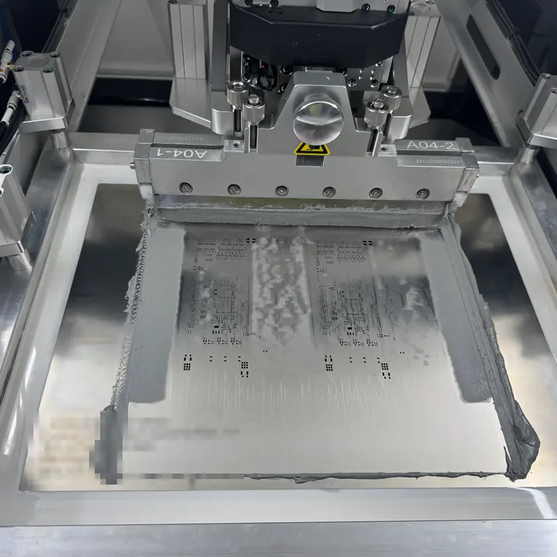
2. Solder Paste Printing Issues
Before components are placed, solder paste is applied to the PCB through a stencil. Warpage affects this process by creating gaps between the stencil and the board surface. If the PCB isn’t flat, the solder paste may not deposit evenly, leading to insufficient or excessive paste on pads. This can result in weak solder joints or bridging during reflow soldering, where excess paste connects adjacent pads and causes shorts.
For instance, a warpage of just 0.2 mm across a board can lead to inconsistent paste thickness, increasing defect rates by up to 10% in some studies. Uniform substrate flatness is essential for achieving consistent paste application.
3. Reflow Soldering Defects
Reflow soldering, where solder paste is melted to form permanent connections, is highly sensitive to PCB warpage. A non-flat board can cause uneven heating across its surface, leading to incomplete solder melting or cold joints. Warpage can also worsen during reflow due to thermal stress, especially if the board design or material isn’t optimized for high temperatures.
One common defect is “tombstoning,” where a component stands upright on one end due to uneven solder reflow caused by board deformation. Another issue is solder joint fatigue, where warped boards create mechanical stress on joints, reducing long-term reliability. For lead-free soldering, which requires higher temperatures (up to 260°C), the risk of warpage-induced defects increases significantly.
How Warpage Affects Overall Production Yield
The combined effect of warpage on pick and place accuracy, solder paste printing, and reflow soldering directly impacts production yield. Warped boards often lead to higher defect rates, requiring rework or even scrapping entire batches. Rework not only increases costs but also risks further damage to components or the board itself. In high-volume production, even a 1% defect rate due to warpage can translate to thousands of dollars in losses over time.
Moreover, warpage can compromise the reliability of the final product. Boards with hidden stress or poor solder joints may fail prematurely in the field, leading to warranty claims and damage to a manufacturer’s reputation. Addressing warpage is therefore not just about assembly efficiency but also about ensuring long-term product quality.
Strategies to Minimize PCB Warpage
Preventing PCB warpage requires a combination of design optimization, material selection, and process control. Here are actionable strategies to maintain substrate flatness and improve automated assembly outcomes:
1. Optimize PCB Design
- Balance Copper Distribution: Ensure copper traces and planes are evenly distributed across all layers of the board. Use dummy copper fills in areas with low trace density to balance thermal expansion.
- Symmetrical Layer Stack-Up: Design the PCB with a symmetrical stack-up to minimize stress. For example, a 4-layer board should have similar material thicknesses and copper weights on corresponding layers.
- Panelization: When designing panels for multiple boards, arrange them to minimize stress during manufacturing. Adding support bars or breakaway tabs can help maintain flatness.
2. Choose the Right Materials
- Low-CTE Materials: Select laminates with a low coefficient of thermal expansion, such as high-Tg FR-4 or polyimide, especially for boards exposed to high temperatures during reflow soldering.
- Moisture-Resistant Options: Use materials with low moisture absorption rates to prevent steam-induced warpage. Proper storage in dry conditions before assembly is also critical.
3. Control Reflow Soldering Profiles
- Gradual Heating and Cooling: Implement a reflow profile with gradual temperature ramps to reduce thermal shock. For example, a preheat stage at 1-3°C per second up to 150°C can help minimize stress.
- Support During Reflow: Use fixtures or carriers to hold the PCB flat during reflow soldering, especially for thin or large boards prone to warpage.
4. Monitor and Test for Warpage
- Inspection Tools: Use tools like shadow moiré or laser scanning to measure warpage before and after reflow. Industry standards suggest keeping warpage below 0.75% of the board’s diagonal length.
- Stress Testing: Simulate thermal cycles during design validation to identify potential warpage risks early in the process.
Why Substrate Flatness Matters for Future Technologies
As electronics continue to shrink in size and increase in complexity, the demand for precise automated assembly grows. Emerging technologies like 5G, IoT, and automotive electronics rely on ultra-fine-pitch components and multi-layer boards, where even minor warpage can cause catastrophic failures. For instance, in a 5G antenna module, component placement accuracy must be within 0.005 mm to ensure signal integrity at high frequencies. Warpage prevention is no longer optional—it’s a critical requirement for staying competitive in modern electronics manufacturing.
Additionally, the shift to lead-free soldering and higher reflow temperatures has made warpage control more challenging. Manufacturers must adapt by investing in better materials, refined processes, and advanced testing to maintain substrate flatness and ensure reliable assembly.
Conclusion
PCB substrate warpage is a significant challenge in automated assembly, impacting pick and place accuracy, solder paste printing, and reflow soldering outcomes. By understanding the causes of warpage—such as material mismatches, thermal stress, and uneven copper distribution—manufacturers can take proactive steps to minimize its effects. Strategies like balanced design, material selection, and controlled reflow profiles are essential for maintaining substrate flatness and achieving high production yields.
At ALLPCB, we’re committed to helping you overcome manufacturing challenges like warpage through expert guidance and high-quality production services. By prioritizing flatness and precision in every step of the process, you can ensure reliable, high-performing PCBs for your applications. Whether you’re working on consumer electronics or cutting-edge tech, addressing warpage is key to success in automated assembly.