ALLPCB


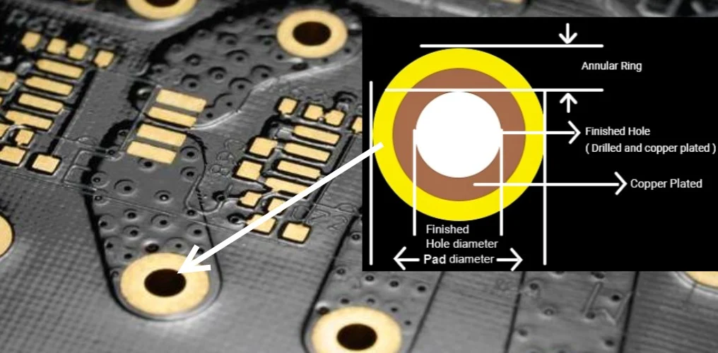
In the world of PCB design, annular rings play a critical role in ensuring reliable connections and structural integrity, especially in through-hole via design. But what exactly is an annular ring, and why is it so important for via design rules, trace connections, and PCB manufacturing? Simply put, an annular ring is the copper area surrounding a drilled hole or via on a printed circuit board (PCB), providing a strong electrical and mechanical connection between layers and components. In this comprehensive guide, we’ll dive deep into the concept of annular rings, their significance in through-hole vias, and best practices to optimize your PCB design for performance and manufacturability.
Whether you're an engineer working on complex multilayer boards or a beginner learning the basics of PCB design, this blog will provide actionable insights and detailed explanations to help you master annular rings in your projects.
What Is an Annular Ring in PCB Design?
An annular ring is the circular copper pad that surrounds a drilled hole or via on a PCB. It acts as a landing area for connecting traces or components to the via, ensuring a solid electrical and mechanical bond. In through-hole via design, the annular ring is especially crucial because it supports the soldering process, where component leads are inserted through the hole and soldered to the pad.
The size and shape of the annular ring directly impact the reliability of the connection. A well-designed annular ring provides enough copper area for soldering or plating, while a poorly designed one can lead to issues like weak connections or manufacturing defects. For instance, if the annular ring is too small, it might not provide sufficient space for solder to adhere properly, leading to potential failures in the circuit.
Why Are Annular Rings Important in Through-Hole Via Design?
Annular rings are vital for several reasons in through-hole via design. They ensure the integrity of the connection between layers of a PCB and provide a stable base for soldering components. Let’s explore their importance in detail:
- Electrical Connectivity: The annular ring connects the via to traces on the PCB, allowing current to flow between layers or components. Without a properly sized ring, the connection might fail, leading to open circuits or intermittent issues.
- Mechanical Strength: During assembly, components are inserted through the via and soldered to the annular ring. A robust ring prevents damage from mechanical stress, such as vibrations or thermal expansion, which could crack the solder joint.
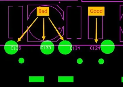
- Manufacturing Reliability: In PCB manufacturing, annular rings help ensure that drilled holes align correctly with the copper pads. Misalignment can cause problems like tangency or breakout, where the via partially or completely misses the pad, compromising the connection.
For high-reliability applications, such as aerospace or medical devices, adhering to strict via design rules for annular rings is non-negotiable. Standards like IPC-6012 often specify minimum annular ring sizes to meet performance and durability requirements.
Key Via Design Rules for Annular Rings
To achieve a reliable PCB design, you must follow specific via design rules related to annular rings. These rules help balance performance with manufacturability. Here are some critical guidelines:
1. Minimum Annular Ring Size
The minimum annular ring size depends on the type of PCB and the manufacturing process. For through-hole vias, the annular ring width is typically measured as the distance from the edge of the drilled hole to the outer edge of the copper pad. A common industry standard is to maintain a minimum annular ring width of 0.2 mm (8 mils) for standard designs, though this can vary based on the PCB class (e.g., Class 2 or Class 3 as per IPC standards).
For high-density designs, where space is limited, you might need to work with smaller annular rings, but this increases the risk of manufacturing defects. Always consult with your PCB manufacturer to confirm their capabilities and ensure your design meets their requirements.
2. Drill-to-Pad Ratio
The drill-to-pad ratio is another critical factor in annular ring design. This ratio compares the diameter of the drilled hole to the diameter of the pad (annular ring included). A typical rule of thumb is to make the pad diameter at least 0.3 mm (12 mils) larger than the drill diameter to ensure a sufficient annular ring width. For example, if your drill size is 0.5 mm, the pad diameter should be at least 0.8 mm.

3. Avoiding Tangency and Breakout
Tangency occurs when the drilled hole is misaligned and touches the edge of the pad, reducing the effective annular ring width. Breakout is a more severe issue where the hole extends beyond the pad, leaving little or no copper for connection. Both issues can lead to unreliable soldering and weak electrical connections.
To prevent tangency and breakout, ensure that your design accounts for manufacturing tolerances. Most manufacturers specify a minimum annular ring width to accommodate potential drilling inaccuracies, often around 0.15 mm (6 mils) or more, depending on their equipment precision.
Annular Rings and Trace Connections
Trace connections to annular rings are another critical aspect of PCB design. Traces are the conductive paths that carry signals or power across the board, and they must connect seamlessly to the annular ring for reliable performance. Here are some best practices for integrating trace connections with annular rings:
- Teardrop Pads: Adding a teardrop shape where the trace meets the annular ring can improve mechanical strength and reduce stress concentration. This design feature helps prevent the trace from breaking due to thermal or mechanical stress during assembly or operation.
- Trace Width Considerations: Ensure that the trace width is appropriate for the current it will carry. For example, a trace carrying 1 Amp of current typically requires a width of 0.5 mm (20 mils) on a standard 1 oz copper layer to avoid overheating. The connection point at the annular ring should not act as a bottleneck for current flow.
- Spacing and Clearance: Maintain adequate spacing between traces and annular rings to prevent short circuits, especially in high-voltage designs. A common clearance rule is 0.2 mm (8 mils) between adjacent conductive elements, though this can vary based on voltage requirements.
By carefully designing trace connections to annular rings, you can enhance the overall reliability of your PCB and minimize the risk of failures in the field.
Annular Rings in PCB Manufacturing
The manufacturing process introduces several challenges for annular rings in through-hole via design. Understanding these challenges can help you create designs that are easier to produce and less prone to defects. Let’s look at some key considerations:
1. Drilling Accuracy
During PCB manufacturing, drilling is one of the most critical steps for creating through-hole vias. Even slight misalignment can result in tangency or breakout, as mentioned earlier. Modern manufacturing equipment can achieve drilling tolerances as tight as ±0.05 mm (2 mils), but this varies by manufacturer. Designing with slightly larger annular rings can provide a buffer for these tolerances.
2. Plating and Soldering
After drilling, through-hole vias are often plated with copper to ensure conductivity between layers. The annular ring must be large enough to support this plating process and provide a robust surface for soldering. If the ring is too small, the plating might not adhere properly, leading to weak connections. A minimum annular ring width of 0.25 mm (10 mils) is often recommended for plated through-holes to ensure reliable results.
3. Thermal and Mechanical Stress
PCBs are subjected to thermal cycling and mechanical stress during assembly and operation. For example, during reflow soldering, temperatures can reach up to 260°C, causing expansion and contraction of the board materials. A well-designed annular ring helps absorb these stresses without cracking or delaminating. Using materials with a low coefficient of thermal expansion (CTE), such as FR-4 with a CTE of around 14-17 ppm/°C, can further improve reliability.

Best Practices for Designing Annular Rings in Through-Hole Vias
To wrap up, let’s summarize some actionable best practices for designing annular rings in through-hole via layouts. These tips will help you create robust, manufacturable designs that perform reliably in real-world applications.
- Adhere to Industry Standards: Follow guidelines from standards like IPC-6012 for minimum annular ring sizes and drill-to-pad ratios. For Class 3 boards (high-reliability applications), stricter rules often apply, such as a minimum annular ring width of 0.05 mm (2 mils) after plating.
- Account for Manufacturing Tolerances: Design with extra margin in your annular ring size to accommodate drilling and alignment inaccuracies. A buffer of 0.1-0.2 mm (4-8 mils) beyond the minimum requirement is often a safe approach.
- Use Design Software Tools: Leverage PCB design software with built-in design rule checks (DRC) to automatically flag potential issues with annular rings, such as insufficient width or tangency risks.
- Collaborate with Manufacturers: Early communication with your PCB manufacturer can help you understand their specific capabilities and constraints. Some manufacturers may offer tighter tolerances or specialized processes that allow for smaller annular rings in high-density designs.
- Test and Validate: For critical applications, consider prototyping and testing your design to verify the performance of annular rings under real-world conditions. Thermal cycling tests and mechanical stress tests can reveal potential weaknesses before full-scale production.
Common Issues with Annular Rings and How to Avoid Them
Even with careful planning, issues with annular rings can arise during PCB design or manufacturing. Here are some common problems and strategies to mitigate them:
- Insufficient Annular Ring Width: This can lead to weak solder joints or poor plating. To avoid this, always design with a width above the minimum specified by your manufacturer, ideally 0.25 mm (10 mils) or more for standard designs.
- Misalignment During Drilling: Misalignment can cause tangency or breakout. Work with manufacturers who use high-precision drilling equipment, and design with larger pads to provide a safety margin.
- Thermal Damage: Excessive heat during soldering can damage the annular ring or surrounding traces. Use thermal relief patterns, such as spokes connecting the ring to large copper planes, to manage heat dissipation effectively.
Conclusion
Annular rings are a fundamental element of through-hole via design in PCBs, directly impacting electrical connectivity, mechanical strength, and manufacturing reliability. By understanding the role of annular rings and adhering to via design rules, you can create robust trace connections and ensure your PCB performs as intended. From maintaining minimum annular ring sizes to accounting for manufacturing tolerances, every detail matters in achieving a high-quality design.
As you work on your next PCB project, keep these guidelines and best practices in mind to optimize your annular ring design. With careful planning and attention to detail, you can avoid common pitfalls and build boards that meet the highest standards of performance and durability. Whether you're designing for consumer electronics or critical industrial applications, mastering annular rings is a key step toward success in PCB manufacturing.