ALLPCB


Overview
To prevent electromagnetic interference (EMI) in high-speed signals, apply the following techniques and design practices.
Key Techniques
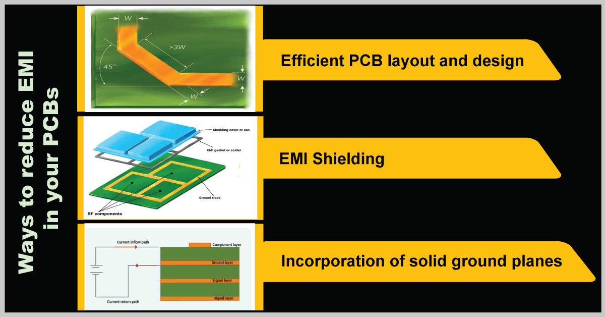
- Ground planning: Proper ground wiring and layout are critical to reducing EMI. Ensure a well-planned ground scheme, minimize return path length, and reduce the loop area of return current.
- Shielding and isolation: Use shielding materials and enclosures to block and isolate high-frequency noise. Consider isolation strategies in the design, such as adding shield layers or isolation walls.
- Ground separation: Separate analog and digital grounds and, where practical, keep them physically apart to reduce mutual interference. This helps prevent high-frequency noise from digital signals from propagating into analog sections via the ground.
- PCB layout: Route high-speed traces away from sensitive analog traces and avoid parallel routing to reduce crosstalk. Thoughtful component placement helps minimize unwanted coupling.
- Minimize return-loop area: Arrange components and routing to reduce the loop area of return currents, which lowers radiated and conducted EMI.
- Control edge rates: Fast signal edges are more likely to generate EMI. Controlling rise and fall times can reduce high-frequency noise emissions.
- Use filters: Apply filters where needed to attenuate high-frequency noise, and ensure proper filtering and damping for high-speed signals.
- Shielded cables and connectors: For long-distance high-speed transmissions, use shielded cables and shielded connectors to isolate and reduce EMI.
Design Guidance
Specific techniques and solutions depend on the application and requirements. When designing and laying out high-speed signal circuits, consult professional engineers and follow electromagnetic compatibility (EMC) guidelines.