ALLPCB


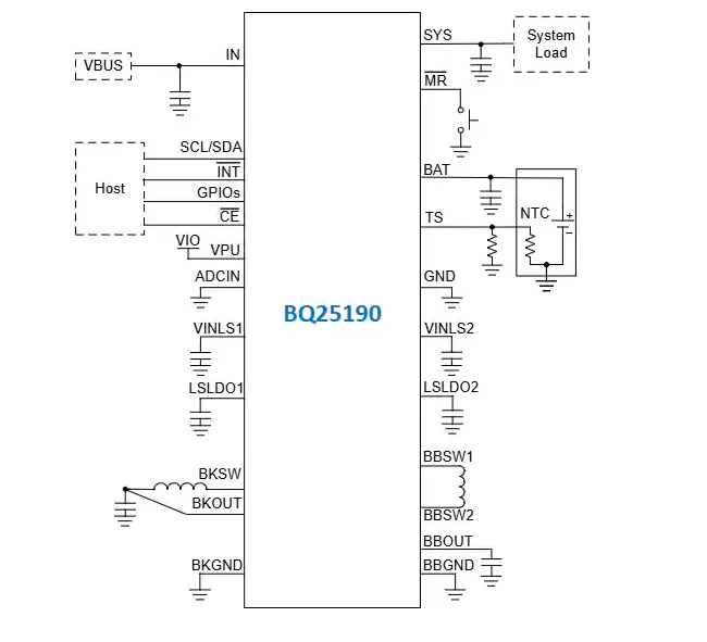
Texas Instruments bq25190 linear battery charger includes common functions for wearable devices, such as a linear charger with a power-path, a buck switching regulator, a buck-boost switching regulator, two LDOs (LDO1 and LDO2), a manual reset (MR) timer, a multichannel analog-to-digital converter (ADC), and four multifunction general-purpose I/Os (GPIOs). This highly integrated battery management device provides low quiescent currents during operation and shutdown to extend battery life.
The integrated charger supports charge currents from 5 mA to 1 A while providing a regulated system voltage (VSYS) to the system. VSYS and other operating parameters such as input current limit, buck regulator output voltage, charge current, buck-boost regulator output voltage, and LDO output voltages are configurable and programmable via the I2C interface. Dynamic power-path management and input-through options allow optimization for weak adapters, and the device can select either adapter or battery to power the system.
Features
- Integrated 1 A power-path linear battery charger
- Operating input voltage range: 3.0 V to 18.0 V
- Input voltage withstand up to 25 V
- Configurable battery regulation voltage, accuracy ±0.5%, range 3.5 V to 4.65 V, 10 mV steps
- Configurable fast charge current: 5 mA to 1 A
- BATFET on resistance: 55 mOhm
- Battery discharge current up to 2.5 A to support heavy system loads
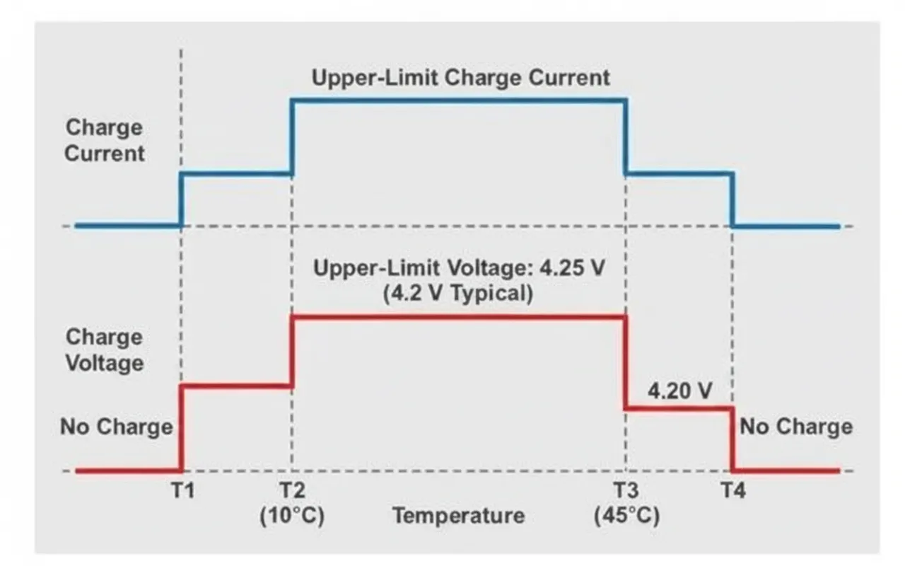
- Fully programmable JEITA charging profile for safe charging across temperature range
- Power-path management for system power and battery charging
- System regulated voltage range: 4.4 V to 4.9 V, with battery tracking and input-through options
- Configurable input current limit
- Dynamic power-path management optimized for weak adapters
- Selectable adapter or battery for system power
- Advanced system reset mechanism
- Integrated buck regulator with I2C and GPIO-programmable DVS output
- System quiescent current: 0.36 uA
- Output voltage: 0.4 V to 1.575 V (12.5 mV steps) or 0.4 V to 3.6 V (25 mV/50 mV steps)
- Output current up to 600 mA
- Ultra-low quiescent current modes
- Battery-mode quiescent current: 2 uA
- Shipping mode battery quiescent current: 15 nA
- Integrated buck-boost regulator with I2C-programmable DVS output
- System quiescent current: 0.1 uA
- Output voltage: 1.7 V to 5.2 V (50 mV steps)
- When VSYS >= 3.0 V and VBBOUT = 3.3 V, output current up to 600 mA
- Integrated I2C-programmable LDOs (LDO1 and LDO2)
- Quiescent current: 25 nA
- Output voltage: 0.8 V to 3.6 V (50 mV steps)
- Output current up to 200 mA
- LDO1 can remain enabled in shipping mode
- Configurable LDO or bypass mode
- Dedicated input pins
- Integrated fault protection for safety
- Input current limit and overvoltage protection
- Battery and integrated rail overcurrent protection
- Battery depletion protection
- Thermal regulation and thermal shutdown
- Integrated 12-bit ADC to monitor input current, BATFET current, input voltage, battery voltage, battery temperature, or external voltage signals
Applications
- Smartwatches and other wearable devices
- Portable medical devices
- Smart trackers
- Retail automation and payment devices
Simplified Schematic