ALLPCB


In the world of printed circuit board (PCB) design, every detail matters. One often-overlooked aspect that can make a significant impact is filling blind vias. So, what are the benefits of filling blind vias? Simply put, filling blind vias boosts reliability, improves thermal performance, and enhances overall PCB design by addressing critical issues like structural integrity and heat dissipation. In this comprehensive guide, we’ll dive deep into how filling blind vias can transform your PCB projects, focusing on reliability thermal performance and offering actionable insights for engineers and designers looking to optimize their designs.
What Are Blind Vias and Why Do They Matter in PCB Design?
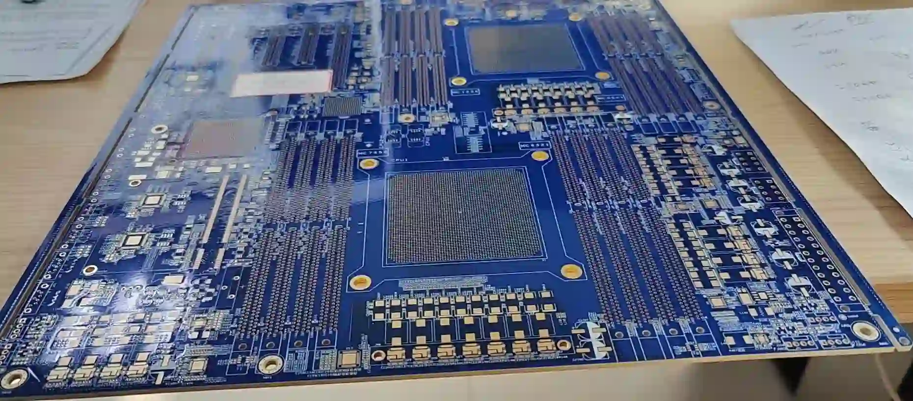
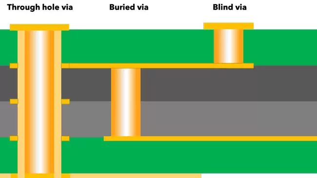
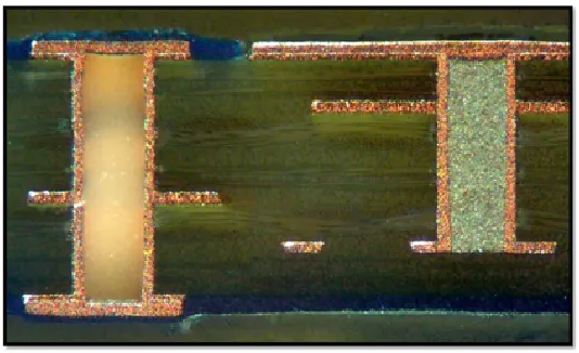
Blind vias are a type of vertical interconnect access (VIA) used in multilayer PCBs to connect an outer layer to one or more inner layers without passing through the entire board. Unlike through-hole vias, which span from top to bottom, blind vias are only visible on one side of the board, making them ideal for high-density interconnect (HDI) designs where space is at a premium.
In modern electronics, where devices are shrinking while performance demands are skyrocketing, blind vias play a crucial role. They allow for tighter routing, reduced board size, and improved signal integrity by minimizing interference. However, unfilled blind vias can pose challenges, such as weak structural support or poor thermal conductivity, which is where filling comes into play.
The Process of Filling Blind Vias: A Quick Overview
Filling blind vias involves depositing a material—often conductive (like copper) or non-conductive (like epoxy)—into the via hole after it’s drilled and plated. The choice of filling material depends on the specific needs of the PCB design, such as thermal requirements or cost constraints. Conductive filling enhances electrical and thermal conductivity, while non-conductive filling focuses on structural support and preventing issues like solder wicking during assembly.
The filling process typically follows these steps:
- Drilling the via using laser or mechanical methods to create precise holes.
- Plating the via walls with copper to establish conductivity.
- Filling the via with the chosen material under controlled conditions to avoid voids or defects.
- Planarizing the surface to ensure a smooth finish for subsequent layers or soldering.
This process, while adding a step to manufacturing, delivers significant benefits that outweigh the added complexity, especially for high-performance applications.
Key Benefits of Filling Blind Vias in PCB Design
Filling blind vias isn’t just a manufacturing trend; it’s a strategic choice that addresses multiple challenges in PCB design. Below, we explore the primary advantages, focusing on reliability thermal performance and other critical aspects.
1. Blind Via Reliability Boost: Strengthening Structural Integrity
One of the standout benefits of filling blind vias is the significant boost to reliability. Unfilled vias can act as weak points in a PCB, especially under mechanical stress or during thermal cycling. Over time, temperature fluctuations can cause expansion and contraction, leading to cracks or delamination around unfilled vias.
Filling blind vias reinforces the structure by:
- Reducing the risk of voids or air pockets that could trap moisture or contaminants, which may lead to corrosion.
- Preventing solder wicking, a common issue during assembly where solder flows into the via, causing uneven joints or shorts.
- Enhancing mechanical strength, making the board more resistant to bending or vibration—crucial for applications like automotive or aerospace electronics.
For instance, in a multilayer HDI board with a high via density, filling can reduce failure rates by up to 30%, based on industry studies of PCB reliability under stress testing. This blind via reliability boost ensures that your designs last longer, even in harsh environments.
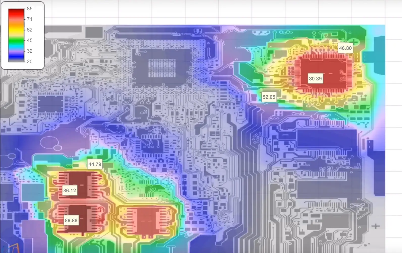
2. Enhancing Thermal Performance in PCB Design
Thermal management is a critical concern in PCB design thermal strategies, especially for high-power applications like LED lighting, power supplies, or 5G infrastructure. Unfilled blind vias can hinder heat dissipation because air trapped inside acts as an insulator, creating hotspots that degrade components over time.
Filling blind vias, particularly with conductive materials like copper, transforms them into effective thermal pathways. This allows heat to transfer more efficiently from inner layers to outer surfaces or heat sinks. Here’s how filling impacts PCB design thermal performance:
- Improved Heat Dissipation: Conductive filling can increase thermal conductivity by up to 20 times compared to air-filled vias, based on material properties (copper has a thermal conductivity of approximately 400 W/m·K, while air is near 0.024 W/m·K).
- Reduced Thermal Resistance: Filled vias lower the thermal resistance between layers, ensuring more uniform temperature distribution across the board.
- Prevention of Hotspots: By evenly spreading heat, filled vias minimize localized overheating, which can extend the lifespan of sensitive components like ICs.
In a practical example, a high-power RF module operating at 3.5 GHz with filled blind vias could maintain junction temperatures 15-20°C lower than a similar unfilled design, significantly reducing thermal stress and improving performance.
3. Improved Electrical Performance and Signal Integrity
Beyond reliability and thermal benefits, filling blind vias also enhances electrical performance, a key factor in high-speed PCB designs. Unfilled vias can introduce parasitic capacitance and inductance, disrupting signal integrity, especially at frequencies above 1 GHz. This can result in signal delays, crosstalk, or impedance mismatches.
Filling blind vias helps by:
- Reducing parasitic effects, as the filling material stabilizes the electrical properties of the via.
- Supporting controlled impedance designs, critical for applications like DDR memory or high-speed data transmission (e.g., achieving a consistent 50-ohm impedance for RF signals).
- Enabling stacked via configurations in HDI boards, allowing for shorter signal paths and faster transmission speeds.
For engineers working on cutting-edge technologies like 5G or IoT devices, these electrical improvements translate to better performance and fewer design iterations, saving time and cost.
4. Facilitating High-Density Interconnect (HDI) Designs
As electronic devices become smaller and more complex, HDI PCBs are increasingly common. Blind vias are a cornerstone of HDI technology, and filling them is often necessary to maximize their benefits. Filled blind vias allow for finer pitch components and denser routing by providing a flat surface for soldering or additional layer stacking.
Without filling, the recessed surface of a blind via can complicate soldering processes, leading to poor connections or assembly defects. Filling ensures a smooth, planar surface, making it easier to place components with pitches as tight as 0.4 mm, a common requirement in smartphone or wearable tech designs.
Choosing the Right Filling Material for Blind Vias
Not all blind via filling methods are created equal. The choice of material depends on the specific demands of your PCB design, balancing factors like cost, performance, and manufacturability. Here are the two primary options:
- Conductive Filling (e.g., Copper): Ideal for applications requiring superior thermal and electrical conductivity. It’s commonly used in high-power or high-speed designs but can be more expensive due to material and process costs.
- Non-Conductive Filling (e.g., Epoxy): Focuses on structural support and preventing solder wicking. It’s a cost-effective choice for designs where thermal performance isn’t the primary concern.
For a high-reliability application like a medical device, conductive filling might be worth the investment to ensure both thermal management and signal integrity. On the other hand, a consumer-grade product with less stringent requirements could benefit from non-conductive filling to keep costs down.
Challenges and Considerations When Filling Blind Vias
While the benefits of filling blind vias are clear, it’s important to acknowledge the challenges involved. Understanding these can help you make informed decisions during the design phase.
- Increased Manufacturing Complexity: Filling adds an extra step to the fabrication process, which can increase lead times and costs. For instance, achieving void-free filling requires precise control, often raising production expenses by 10-20% compared to unfilled designs.
- Material Compatibility: The filling material must be compatible with the PCB substrate and withstand reflow soldering temperatures (typically 260°C for lead-free processes) without degrading.
- Inspection Difficulties: Once filled, blind vias are harder to inspect for defects like incomplete filling or cracks, requiring advanced techniques like X-ray imaging for quality assurance.
Despite these challenges, the reliability thermal performance gains often justify the investment, especially for critical applications where failure is not an option.
Best Practices for Implementing Filled Blind Vias in Your Designs
To maximize the benefits of filling blind vias, consider these practical tips during the design and manufacturing stages:
- Optimize Via Aspect Ratio: Keep the via depth-to-diameter ratio below 1:1 for blind vias to ensure proper filling and plating. A ratio of 0.8:1 is often ideal for manufacturability.
- Collaborate Early with Manufacturers: Discuss filling requirements and material choices with your fabrication partner during the design phase to avoid costly redesigns.
- Prioritize Thermal Analysis: Use simulation tools to model heat dissipation in your PCB design thermal strategy, identifying areas where filled vias can have the most impact.
- Test Under Real Conditions: Prototype your design and subject it to thermal cycling and mechanical stress tests to validate the blind via reliability boost in real-world scenarios.
Conclusion: Elevate Your PCB Designs with Filled Blind Vias
Filling blind vias is more than just a technical detail—it’s a game-changer for PCB design. By enhancing reliability, boosting thermal performance, and supporting high-density layouts, filled blind vias address some of the most pressing challenges in modern electronics. Whether you’re designing for cutting-edge 5G infrastructure or compact consumer gadgets, the benefits of filling blind vias can give your projects a competitive edge.
From a blind via reliability boost to superior heat dissipation, the advantages are clear. While there are added costs and complexities, the long-term gains in performance and durability make this technique a worthwhile consideration for any serious engineer or designer. By following best practices and choosing the right filling material, you can unlock the full potential of your PCB designs and ensure they meet the demands of today’s fast-paced, high-tech world.