ALLPCB


Overview
Although SRAM remains the dominant on-chip memory, advanced process nodes introduce new challenges for its use. SRAM has long been the preferred memory for low-latency, high-reliability applications, especially in AI, but limited scalability is creating trade-offs across power, density, and performance that affect overall system design.
SRAM vs DRAM: fundamental trade-offs
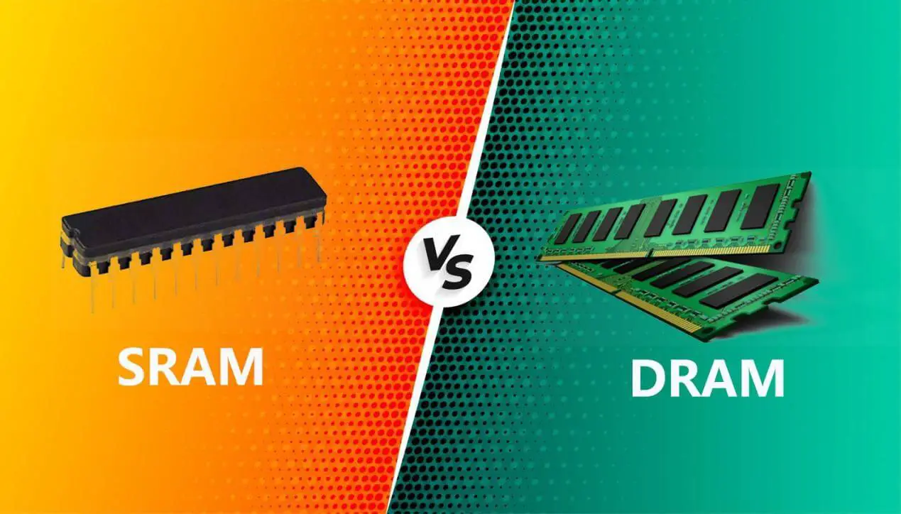
SRAM cells typically use six transistors, providing faster access than DRAM at the cost of greater area and higher read/write power. DRAM uses a single-transistor, single-capacitor cell that is denser and cheaper, but requires periodic refresh due to charge leakage, which can impact latency and power. For over six decades, SRAM has been prioritized where low latency and reliability are critical, such as for caches and embedded memories.
Power and performance pressures at advanced nodes
SRAM scaling has lagged behind logic scaling, undermining expected power and performance benefits. Historically, reducing gate length and gate oxide thickness enabled lower VDD and improved short-channel control, which helped both leakage and dynamic power. Recent nodes have seen less oxide and VDD scaling, while device geometry shrinkage has thinned metal interconnects, increasing parasitic resistance and RC delay. As AI workloads demand more on-chip memory bandwidth, these effects contribute to rising SRAM power and degraded performance.
When designers cannot integrate enough SRAM to satisfy processor core working sets, data must be moved from farther memory tiers. Migrating data between SRAM and DRAM consumes additional power and increases access latency, which reduces system performance. If current trends continue through further node transitions, the situation could worsen rather than improve.
Architectural responses
Because caches can occupy a disproportionately large portion of a chip, several architectural strategies are being pursued:
- 3D stacking of SRAM, as exemplified by AMD's 3D V-Cache, where additional SRAM dies are stacked on top of the CPU to increase available cache capacity. This increases cost but provides more on-die cache.
- Multi-level cache hierarchies that combine small private L1/L2 caches with larger shared last-level caches (LLC) to improve overall utilization across many cores.
Error correction and reliability
Reduced SRAM scaling also raises reliability concerns. Error-correcting codes and related mitigation techniques are becoming more common, and may be required in safety-critical domains such as automotive systems.
Alternative memory technologies and chiplet approaches
Designers are exploring ways to use less on-chip SRAM. If higher latency can be tolerated, larger capacity can be moved to DRAM or HBM at higher cost. Emerging embedded non-volatile memories, such as MRAM and ReRAM, offer smaller cell area than SRAM. Although these technologies can reduce cell footprint—overall cell area including peripherals can be significantly smaller than SRAM—their write speeds remain much slower than SRAM, limiting use cases.
If physics prevents further SRAM miniaturization, system architects may combine advanced-node logic with older-node SRAM via chiplets. This allows logic to benefit from improved PPA on the most advanced process node while placing dense SRAM on more cost-effective, mature nodes with higher yields. Multi-chip integration aligns with the trend of producing each circuit on an optimal node and then packaging chips together.
Interconnects and system-level changes
New layouts and high-speed interconnect protocols such as UCIe and CXL are attracting interest. Larger AI workloads scale memory with compute, and mismatched scaling rates across components can create different system bottlenecks. Growing AI workloads also increase the number of required processors, sometimes exceeding reticle size limits and motivating multi-chip systems interconnected with high-bandwidth links. Consequently, multi-chip solutions are becoming inevitable for some AI workloads.
System-technology co-optimization can also help in limited scenarios. For example, some AI training workflows use data that is read once, allowing software and chip architectures to bypass conventional cache hierarchies and reduce on-chip caching requirements.
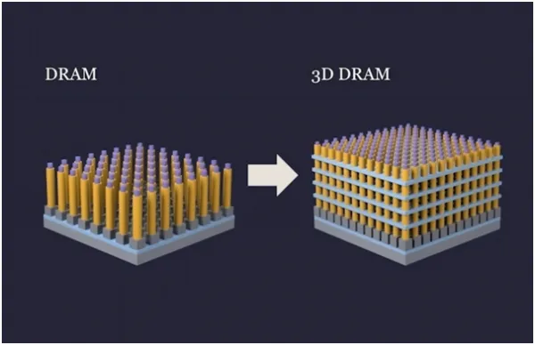
Example: DRAM-based 3D stacks
Some vendors are rethinking memory architecture with 3D-stacked DRAM approaches that provide dense storage connected through through-silicon vias. These provide a cost advantage because DRAM cells avoid the six-transistor overhead of SRAM. Such stacks can replace SRAM at certain cache levels by offering higher density and scalable I/O bandwidth, trading off latency characteristics and implementation complexity. Prototype efforts are ongoing, with projected production timelines dependent on vendor roadmaps.
Conclusion
Changes are likely to be incremental at first. Designers will continue to balance cache size against cost and performance. If SRAM becomes more expensive or scarce, systems will accept some performance loss or compensate with greater DRAM bandwidth. Over time, persistent trends could drive more radical architectural shifts and wider adoption of chiplet-based designs, alternative memory technologies, and new interconnects. Complete replacement of SRAM appears unlikely in the short term, but a long-term transition would require corresponding changes in architecture and system software.