ALLPCB


Introduction
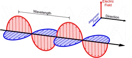
Electrostatic discharge (ESD) is the rapid transfer of charge between objects at different electrostatic potentials. ESD can cause excessive electrical stress to electronic components and systems, disrupting circuit function and causing malfunction or failure. The physical mechanisms involved in ESD are complex, so analytical hand calculations rarely yield precise discharge levels or protection device performance. Physical prototyping and board respinning are time-consuming and costly, so simulation is useful to predict ESD behavior and evaluate protection strategies before production. The following case study shows an ESD simulation workflow using Sigrity Speed2000 and how it can help engineers analyze ESD effects prior to fabrication.
1. Case Description
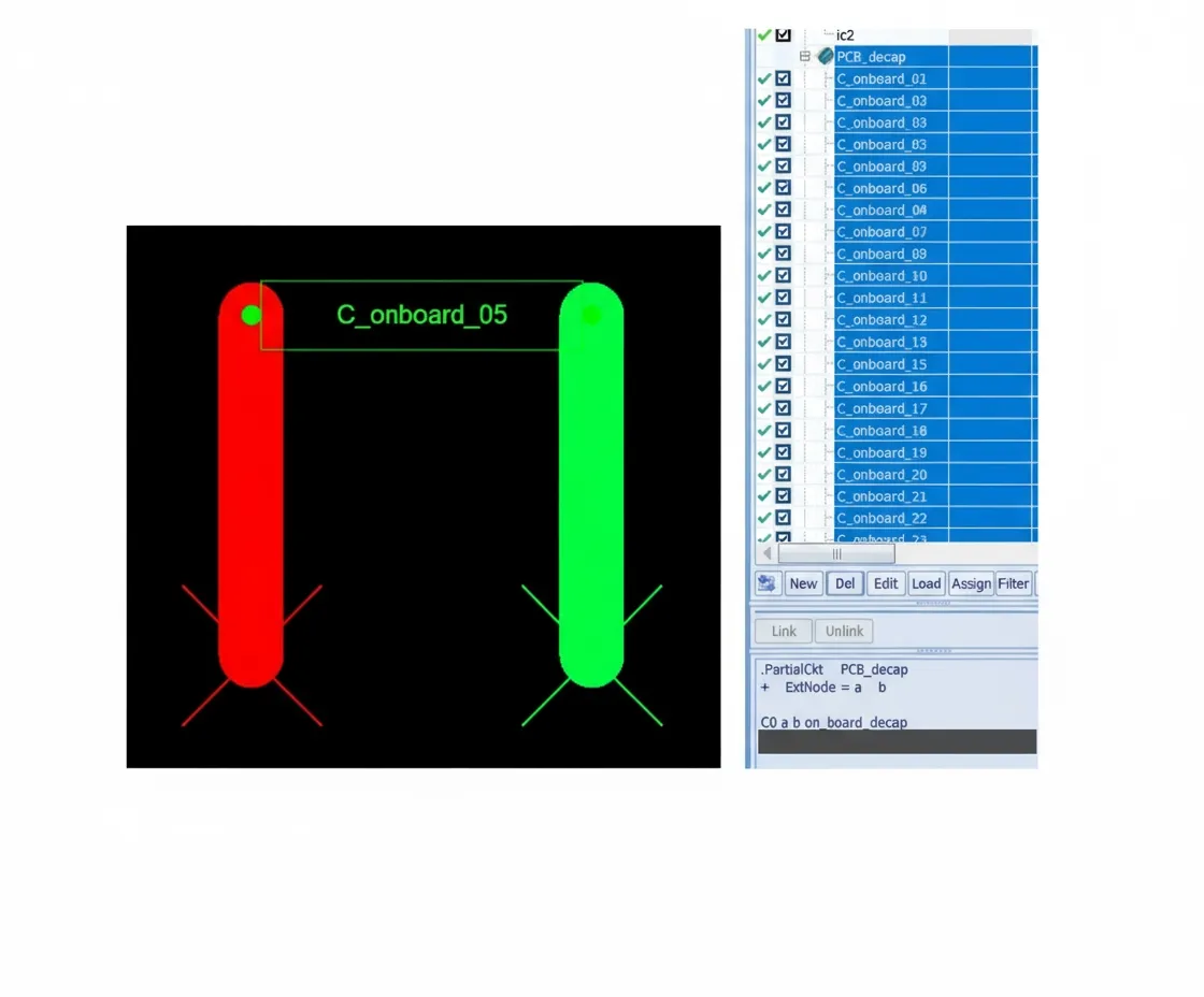
A four-layer PCB is used in this case. Trace1 and trace2 connect to top-layer chips ic1 and ic2 respectively. The signal networks are t0 and t1. Power and ground networks are VDD and GND. The bottom layer includes multiple decoupling capacitors.
2. Simulation Approach
Step 1: Use an ESD gun model to analyze voltage waveforms on chip signal and power pins with no ESD protection applied. The discharge affects not only the directly discharged trace1, but also couples to power planes and adjacent trace2, so ic2's signal and power are included in the simulation.
Step 2: Evaluate the impact of adding decoupling capacitors and assess the effect of TVS devices.
Step 3: Extract voltages on chip pins as noise sources and analyze how ESD-induced noise affects signals and power, including potential loss of signal recognizability.
3. ESD Gun Model
The ESD gun model is based on IEC-61000-4-2 or EN-61000-4-2 (HBM human-body model). EMC standards define the ESD gun output by current waveform. The output has two segments: the first segment has a very short rise time (0.7-1 ns) and a high peak current (3.75 A/kV), representing the instantaneous discharge of charge accumulated on the arm; the second segment (10-60 ns) represents the release of body-accumulated charge.
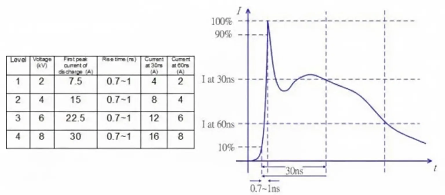
The software provides a default gun model that reproduces this current waveform. Engineers can use the default model or edit model parameters and topology in the edit model interface to define a custom ESD gun model.
4. Simulation Process
Step 1 — Simulation without ESD Protection
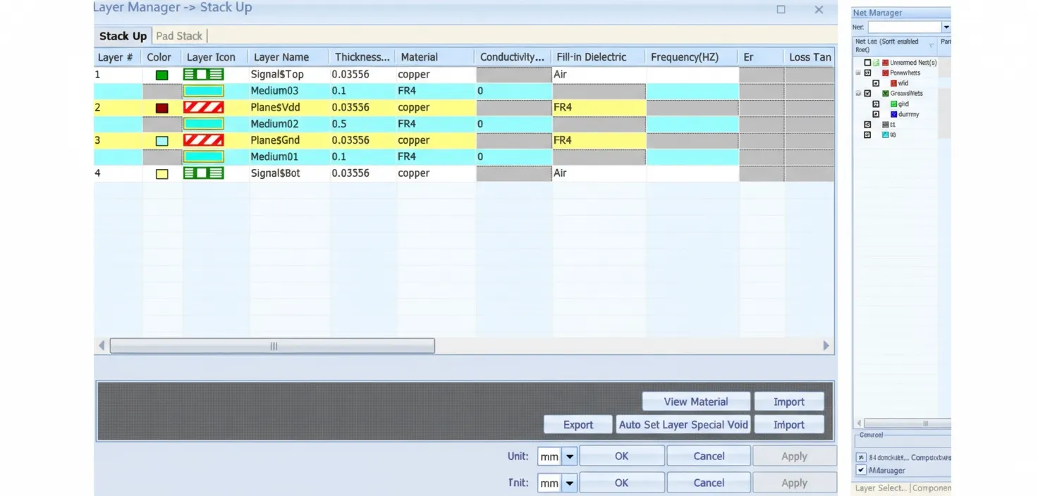
Perform layout stackup checks and network selection.
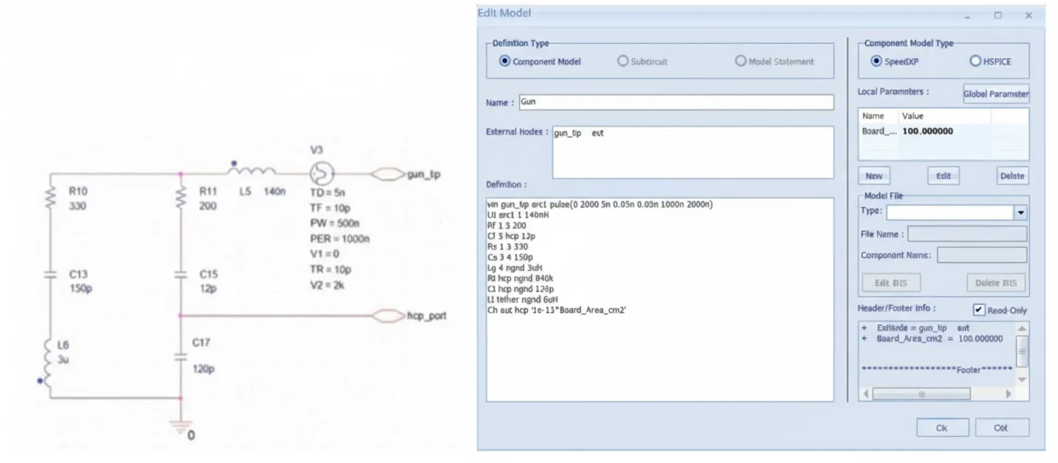
Add the ESD gun model (default parameters used here) and place the gun at the discharge location in the layout.
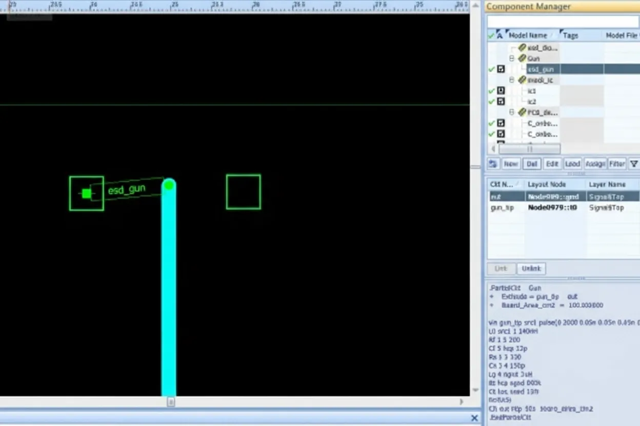
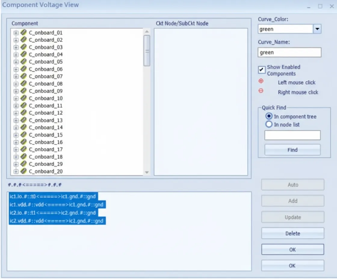
Add voltage observation points on the power and signal pins of ic1 and ic2.
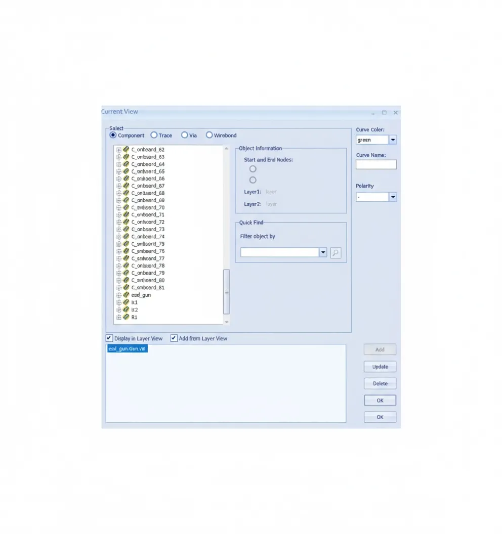
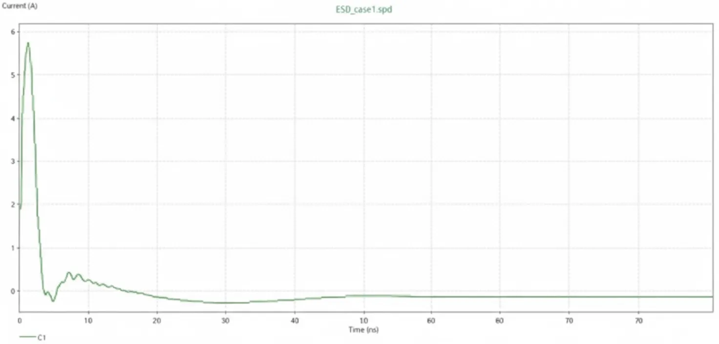
Add a current observation point at the ESD gun to verify the model current waveform.
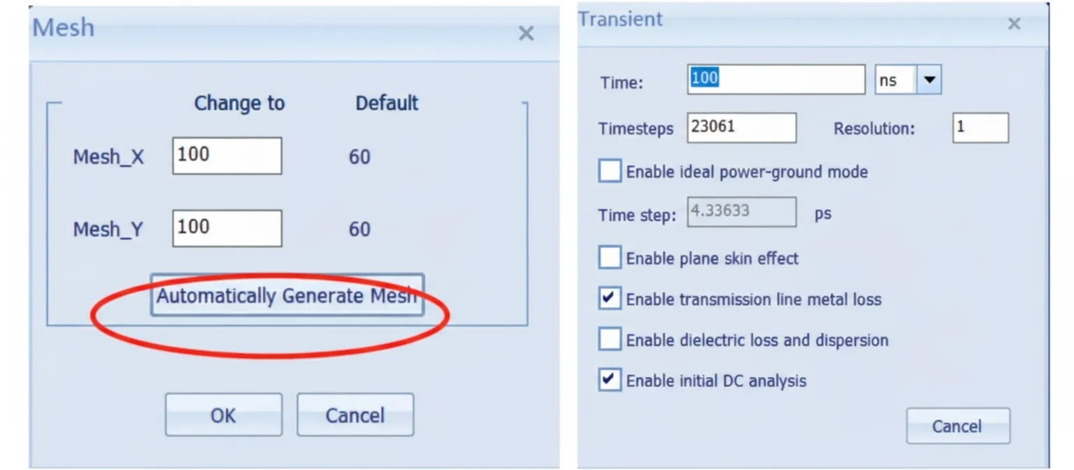
Speed2000 uses a 3D time-domain FDTD solver, so mesh generation is required. Use automatic mesh generation and set simulation time and other options.
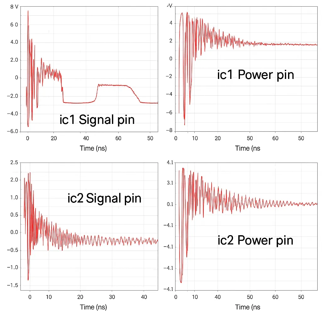
Simulation results show that without ESD protection the voltage at ic1 signal pin (direct discharge) can reach about 14 V, and large ringing follows the initial discharge. These oscillations can mask normal signal levels. Coupled noise at ic2's signal pin is about 3 V, and coupled noise on the two chips' power pins via plane coupling is roughly 2.5 V.
The ESD gun current waveform was validated against the standard.
Step 2 — Simulation with ESD Protection
Enable all decoupling capacitors (equivalent to adding ESD capacitors) and observe the results.
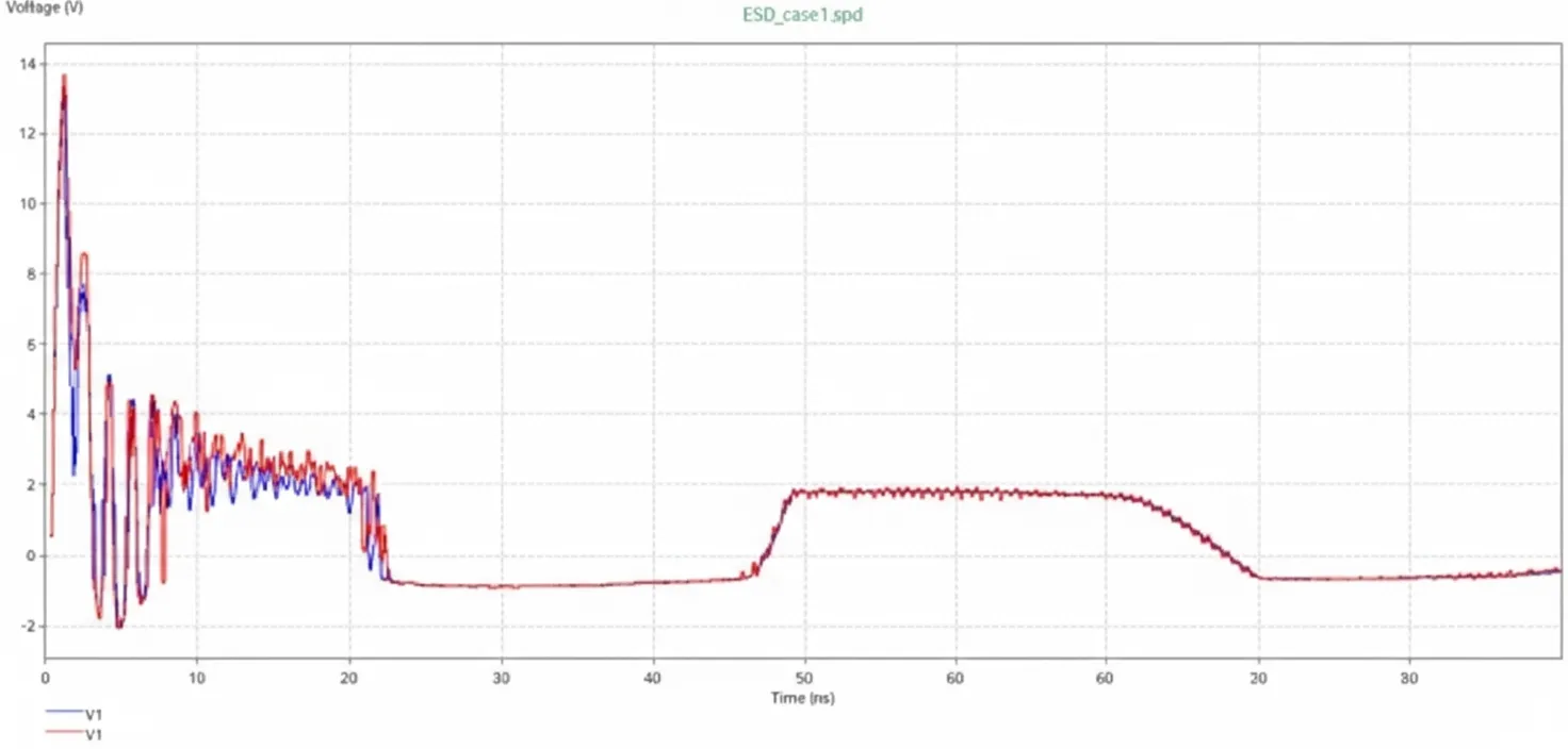
The blue curve shows results with decoupling capacitors, while the red curve shows results without them. Adding decoupling capacitors reduced discharge noise amplitude at the ic1 pin by about 1 V and mitigated ringing.
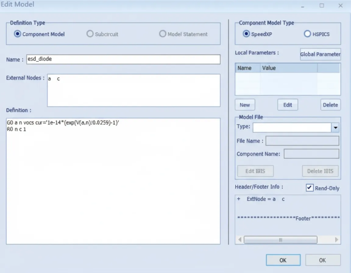
Next, add a TVS device near the discharge location using the software's default model and evaluate its effect.
The TVS model description is shown here.
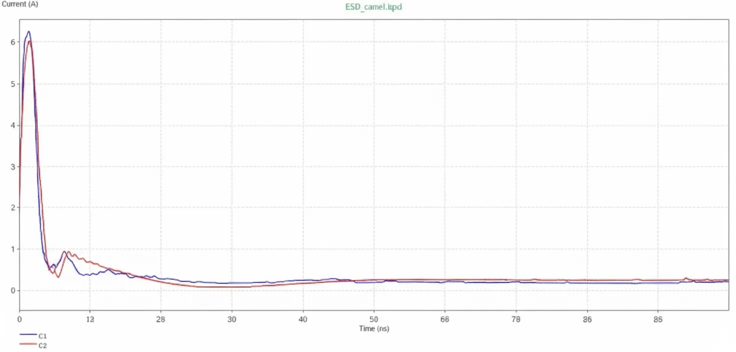
The discharge current waveform with and without the TVS is shown below. Blue is with TVS, red is without. Adding the TVS has little effect on the current waveform at the discharge location.
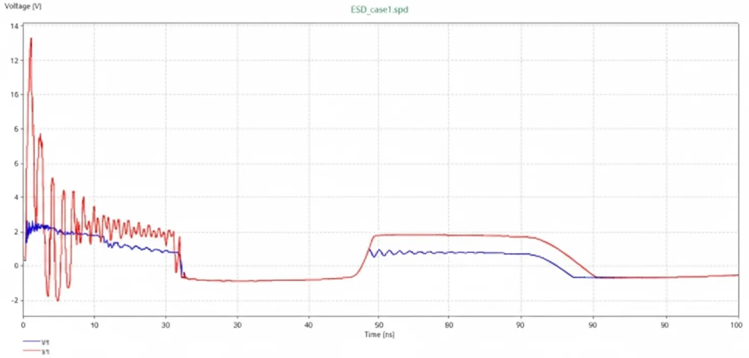
The noise at the ic1 pin is shown next: blue is with TVS, red is without. Adding the TVS reduces the chip-end discharge noise significantly in this case, from about 14 V down to approximately 2 V, bringing the noise to a controllable level.
Step 3 — SI Impact of ESD Noise
Use Speed2000's IBIS simulation to evaluate how discharge noise affects signal integrity.
The signal source model used in this case is a 500 Mbps PRBS pattern.
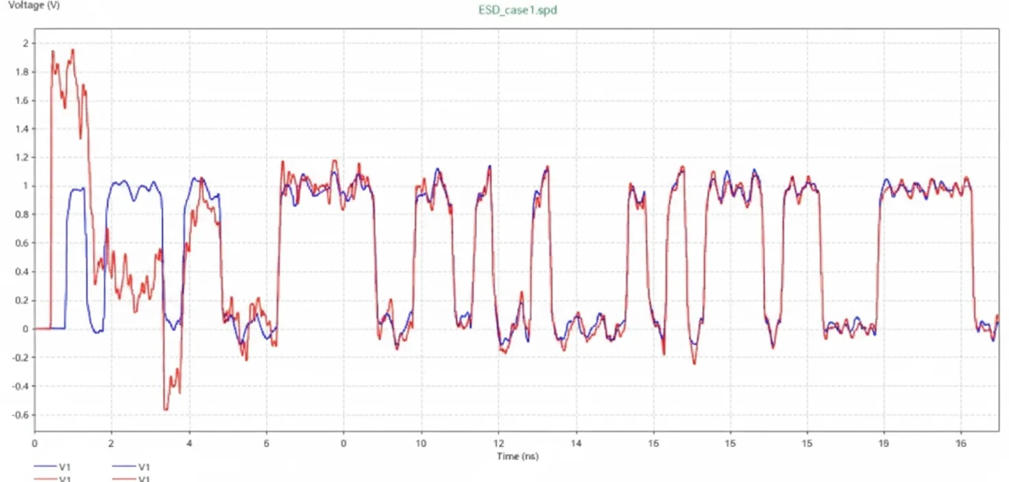
Simulation results at 500 Mbps show the receiver waveform at ic1 with and without the TVS. The discharge noise causes severe waveform distortion and can impair level detection. Adding the TVS restores the waveform and mitigates the problem.
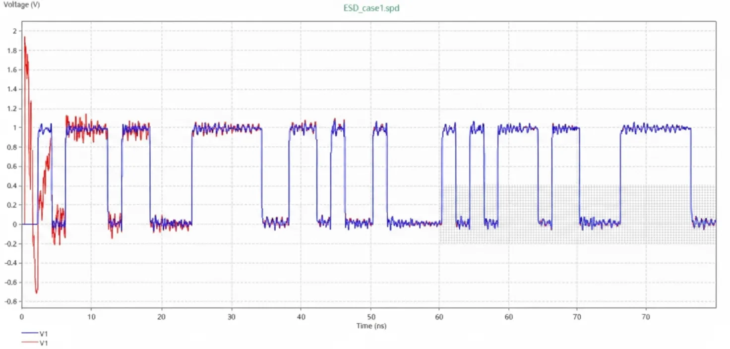
Raising the data rate to 2 Gbps increases the impact of discharge noise. The comparison below shows the receiver waveform at ic1 with and without TVS at 2 Gbps, again demonstrating the protective effect of the TVS.
5. Conclusions
This case study demonstrates how Sigrity Speed2000 can be used for ESD simulation and analysis. The ESD workflow allows estimation of discharge voltages, provides an ESD gun excitation model for discharge simulation, and supports adding protection devices such as decoupling capacitors and TVS diodes to evaluate protection effectiveness. Combined with IC I/O models or defined signal sources, the tool can assess the impact of ESD-generated noise on signal integrity, helping schematic, PCB, and simulation engineers make informed decisions about ESD vulnerability and protection design before production.