ALLPCB


Introduction
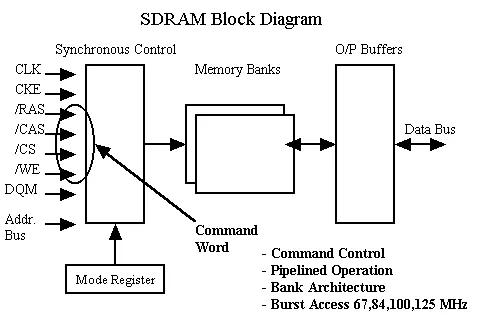
SDRAM (synchronous dynamic random-access memory) is synchronous because its operation is driven by an external clock; internal command transmission and data transfers are timed to that clock. It is dynamic because stored data is held in capacitors that leak charge and therefore require periodic refresh to retain data. It is random-access because reads and writes can target arbitrary addresses rather than being strictly sequential.
1. Notes
The following points collect details that are commonly misunderstood. If some concepts are not clear, review basic SDRAM terminology first.
1.1 Burst Length
Burst transfer: after a row is activated, specifying a starting column and a burst length causes the device to automatically perform sequential read/write accesses to that number of column locations without the controller supplying column addresses for each access.
Reads and writes to SDRAM are burst-oriented; the burst length (BL) is programmable. Burst length defines how many column locations a single read or write command can access.
Burst types may be Sequential or Interleaved; burst length options are 1, 2, 4, 8, or full page (continuous). Sequential burst type also supports continuous page bursts. Continuous page bursts can be terminated with the BURST TERMINATE command to produce arbitrary burst lengths.
Reserved states should not be used because they may produce undefined behavior or be incompatible with future device versions.
When a read or write command is issued, a block of columns equal to the burst length is selected. All accesses for that burst occur within that block, so the burst wraps within the block at boundaries.
1.2 Auto Refresh (AR) and Self Refresh (SR)
Refresh operations are either Auto Refresh (AR) or Self Refresh (SR). Both methods do not require external row addresses, because the device internally generates the row addresses for refresh.
For AR, the SDRAM contains an internal row-address generator (refresh counter) that issues row addresses sequentially. Since refresh touches all cells in a row, no column addressing is required; CAS is asserted before RAS, so AR is sometimes called CBR (CAS Before RAS) refresh.
Refresh impacts all banks: during refresh, all banks are inactive, and for the PC133 timing example each refresh occupies 9 clock cycles, during which normal commands must wait. Each row is refreshed at least once every 64 ms. Refresh overhead reduces DRAM performance compared with static RAM, which does not require periodic refresh.
SR is used to preserve data while the system clock is inactive, for low-power states such as suspend-to-RAM. Entering SR is performed by issuing AR while deasserting CKE; the device then refreshes based on its internal clock. During SR, external signals other than CKE are ignored. Reasserting CKE exits SR and returns to normal operation.
2. Operation
The following describes operation using the IS42S16320D as an example. Verilog code referenced in the original documentation is not included here.
2.1 Timing
Every command execution and data transfer must meet the device timing parameters. To satisfy command setup time (tCMS) and hold time (tCMH) for command latching, the SDRAM clock (SD_clk) is typically phase-shifted or inverted relative to the system clock, or generated by a divide mechanism.
Example: system clock clk = 100 MHz.
2.2 Refresh Interval
The maximum retention interval for SDRAM cell data is 64 ms. With 8K rows per bank, the maximum interval between refreshes for the same row is 64 ms / 8192 ≈ 7.8 μs. To provide margin and leave more time for read/write, a refresh period of 7.7 μs is used in this design.
If a refresh is required during a read or write, the sequence is PRECHARGE -> IDLE -> REFRESH. Ensure that:
refresh time + required wait time ≤ 7.8 μs.
For a read, the required wait time includes: activate time (tRCD) + CAS latency (tCL) + time to read a page + precharge time (tRP).
For a write, the required wait time includes: activate time (tRCD) + time to write a page + precharge time (tRP).
Implementation strategy: combine a periodic timer and manual control. A 7.7 μs timer runs continuously; if it expires, perform refresh. If a refresh request arrives before the timer expires, perform manual refresh and reset the timer. This allows refresh to occur after reads/writes while ensuring periodic refresh if the controller is idle.
2.3 Full Page Operations
For high-throughput large transfers use page-mode operations with burst length set to full page. In page mode the SDRAM must be stopped with a burst stop or burst terminate command.
To make page-mode transfers flexible, use an external register where software writes the desired byte count before starting a transaction. The controller monitors that byte count and issues a burst terminate at the appropriate time. This supports adjustable transfer sizes from 1 to 256 bytes for greater versatility.
2.4 State Machine
Refer to the IS42S16320D state diagram and understand each state and the transition conditions carefully when designing the controller state machine.
3. Detailed Operations
Primary device states include: power-up initialization, idle, read, write, and refresh.
3.1 Initialization
On power-up the device requires a fixed initialization sequence described in the datasheet.
Key steps:
- Power-up delay: After power-on the device requires a delay (typically 100 μs for this device; some other DRAMs specify 200 μs). During this delay issue NOP or COMMAND INHIBIT. CKE must be driven active (high) to enable the clock input.
- Precharge: After the power-up delay, issue Precharge All to close any open rows and prepare banks for activation.
- Auto refresh: After tRP (PRE to ACT) minimum 15 ns, issue the first Auto Refresh. After tRC (REF to REF / ACT to ACT) minimum 60 ns, issue the second Auto Refresh.
- Mode register set: After the second Auto Refresh and a tRC interval, program the mode register using the A9-A0 address pins to select operating mode parameters.
- Initialization complete: After tMRD (Mode Register Program Time) 14 ns, the device is ready for ACTIVE commands and normal operation.
3.2 Row Activation
Before reads or writes from a bank, issue ACTIVE to open the target row. After ACTIVE, wait tRCD (Active Command to Read/Write Command Delay) 15 ns before issuing Read or Write.
Activating different rows in the same bank requires at least six clock cycles between activations. Activating rows in different banks requires at least two cycles, enabling parallelism across banks.
3.3 Write Data
The first write data word aligns with the WRITE command. After writing the configured burst length, DQ lines return to high-Z and the device stops accepting data. For full-page writes, without a burst terminate the burst will wrap and begin overwriting from the start of the block.
If a PRECHARGE is required during a write, reserve tDPL (14 ns, aligned to the last data rising edge). The write is interrupted and the precharge occurs after tRP. DQM can be asserted to mask data input during an interrupt. Note: DQM masks internal buffers and does not immediately suppress previously buffered output; ensure correct timing when asserting and deasserting DQM. DQM must be deasserted before the WRITE command arrives; otherwise input data will be ignored.
3.4 Read Data
When issuing a new command during a continuous read, the command issue time must ensure that the last expected read data arrives before CAS latency - 1 cycles relative to the command. In practice, write commands during a read-to-write transition should be delayed by one cycle to avoid I/O contention, since the device driving the input data may go high-Z before the SDRAM DQs return to high-Z. In this case, include at least a single-cycle delay between the last read data and the WRITE command.
To avoid I/O conflicts assert DQM in advance. Typically assert DQM three cycles before a WRITE command to block input; remember DQM does not immediately suppress output, only internal buffers.
4. Open Questions
The typical refresh execution described is: after completing read/write in the same bank and row, issue PRECHARGE then perform two Auto Refresh cycles. Is it possible to perform refresh without a prior PRECHARGE?
In the state machine the CBR refresh path shows automatic transition to PRECHARGE. How should that be interpreted?