 ALLPCB


If you're looking to enhance your PCB designs for high-speed applications, backdrilling is a powerful technique to consider. This process removes unused portions of via stubs, improving signal integrity and reducing interference in high-speed circuits. In this comprehensive guide, we'll dive deep into what backdrilling is, why it matters for PCB designs, and how it can optimize performance by tackling issues like via stubs and signal degradation. Whether you're a seasoned engineer or new to high-speed design, this blog will provide actionable insights to elevate your projects.
What Is Backdrilling in PCB Designs?
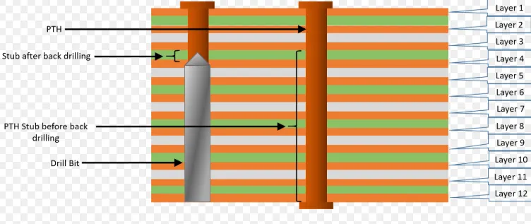
Backdrilling, also known as controlled depth drilling, is a manufacturing technique used in printed circuit board (PCB) fabrication. It involves drilling out the unused portion of a through-hole via from the opposite side of the board after the initial plating process. These unused sections, often called via stubs, can negatively impact signal integrity, especially in high-speed designs operating at frequencies above 1 GHz.
In a typical multilayer PCB, vias connect different layers. However, when a via extends beyond the layers it needs to connect, the leftover stub acts like an antenna, causing signal reflections, crosstalk, and impedance mismatches. Backdrilling removes this stub, ensuring cleaner signal transmission and better overall performance.
Why Backdrilling Matters for High-Speed PCB Designs
In high-speed PCB designs, maintaining signal integrity is critical. As data rates increase—often exceeding 10 Gbps in modern applications—small imperfections in the design can lead to significant performance issues. Via stubs are a common culprit, as they introduce unwanted capacitance and inductance, leading to signal distortion.
For example, a via stub in a 12-layer PCB operating at 5 GHz can cause a signal reflection that degrades the bit error rate (BER) by as much as 10^-6 or more. Backdrilling eliminates this problem by physically removing the stub, reducing signal loss and ensuring that impedance remains consistent along the transmission path, often targeting a standard 50-ohm impedance for high-speed signals.
Beyond signal integrity, backdrilling also minimizes electromagnetic interference (EMI) and crosstalk between adjacent traces. This is especially important in dense designs where high-speed signals run close to each other, such as in telecommunications equipment or data center hardware.
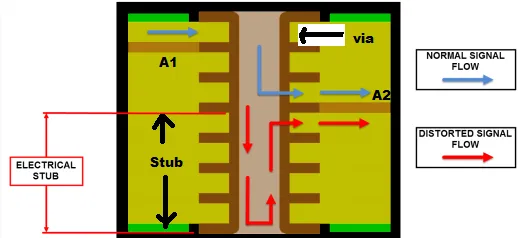
How Via Stubs Affect Signal Integrity
Via stubs are essentially unused segments of a via that extend beyond the connected layers. In high-speed designs, these stubs act as resonant structures, reflecting signals back into the transmission line. This reflection creates noise, distorts the signal waveform, and can even cause data errors in digital circuits.
The impact of via stubs becomes more pronounced as signal frequency increases. At 1 GHz, a stub as short as 0.5 mm can cause noticeable signal degradation. By 10 GHz, even a 0.1 mm stub can wreak havoc on signal quality. The rule of thumb is that stubs longer than 1/10th of the signal wavelength will likely cause issues, making backdrilling a necessity for modern high-speed applications.
The Backdrilling Process: Step by Step
Understanding the backdrilling process can help you design PCBs that are compatible with this technique. Here's how it typically works in manufacturing:
- Initial Via Drilling: The PCB is first drilled with through-hole vias to connect the necessary layers during the design phase.
- Plating: The vias are plated with conductive material (usually copper) to ensure electrical connectivity between layers.
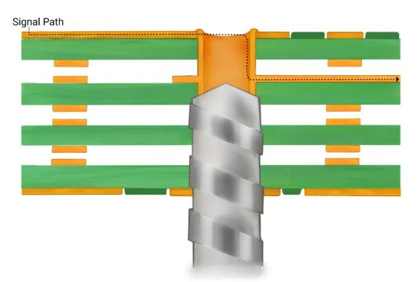
- Backdrilling Setup: Using precise CNC drilling machines, the manufacturer identifies the vias that require stub removal based on the design files.
- Controlled Depth Drilling: A larger drill bit removes the unused portion of the via from the opposite side of the board, stopping just before the active signal layer to avoid damaging the connection.
- Inspection: The board undergoes quality checks to ensure the backdrilling depth is accurate and no debris or damage affects the via's functionality.
This process requires high precision, as over-drilling can sever critical connections, while under-drilling may leave residual stubs. Modern fabrication tools can achieve depth tolerances as tight as ±0.05 mm, ensuring reliable results even in complex multilayer boards.
Key Benefits of Backdrilling in PCB Designs
Implementing backdrilling in your PCB designs offers several advantages, particularly for high-speed applications. Here are the most significant benefits:
- Enhanced Signal Integrity: By removing via stubs, backdrilling minimizes signal reflections and maintains consistent impedance, ensuring cleaner data transmission at speeds above 5 Gbps.
- Reduced Crosstalk: Eliminating stubs lowers the risk of interference between adjacent high-speed signals, which is crucial in dense PCB layouts.
- Lower EMI: Stubs can act as antennas, radiating electromagnetic noise. Backdrilling reduces EMI, helping your design meet strict regulatory standards.
- Improved Design Flexibility: With backdrilling, you can use through-hole vias in high-speed designs without worrying about stub-related issues, simplifying routing in multilayer boards.
- Cost-Effective for Performance: While backdrilling adds a manufacturing step, it often eliminates the need for more expensive alternatives like blind or buried vias, balancing cost and performance.
These benefits make backdrilling a go-to solution for industries like telecommunications, aerospace, and computing, where high-speed signal integrity is non-negotiable.
Applications of Backdrilling in High-Speed Designs
Backdrilling is widely used in applications where signal integrity directly impacts performance. Some common use cases include:
- Data Centers and Servers: High-speed interconnects in server boards often operate at 25 Gbps or higher, requiring backdrilling to ensure error-free data transfer.
- Telecommunications: Equipment like routers and switches handling 10 Gbps or 40 Gbps signals rely on backdrilling to maintain signal quality over long distances.
- Automotive Electronics: Advanced driver-assistance systems (ADAS) and infotainment systems use high-speed signals that benefit from stub-free vias.
- Medical Devices: High-frequency imaging and diagnostic equipment require precise signal transmission, making backdrilling essential.
In each of these scenarios, backdrilling ensures that PCB designs meet the stringent performance demands of modern technology.
Design Tips for Implementing Backdrilling
To maximize the benefits of backdrilling in your PCB designs, consider the following best practices during the design phase:
- Identify High-Speed Signals Early: Determine which vias carry high-speed signals (above 1 GHz) and mark them for backdrilling in your design files. This helps the manufacturer execute the process efficiently.
- Optimize Via Placement: Place vias strategically to minimize stub length even before backdrilling. Route high-speed signals on top layers when possible to reduce via depth.
- Specify Drill Depth: Work closely with your fabrication partner to define precise backdrilling depths, ensuring they stop just below the last connected layer (typically within 0.1 mm tolerance).
- Use Simulation Tools: Leverage signal integrity simulation software to model the impact of via stubs and verify the effectiveness of backdrilling in your design. Target impedance mismatches below 5% for optimal results.
- Account for Manufacturing Limits: Backdrilling works best with vias larger than 0.3 mm in diameter due to drill bit constraints. Smaller vias may require alternative solutions like microvias.
By incorporating these tips, you can ensure that your PCB designs are ready for backdrilling and achieve the best possible performance in high-speed applications.
Challenges and Limitations of Backdrilling
While backdrilling offers significant advantages, it's not without challenges. Being aware of these limitations can help you plan your designs more effectively:
- Increased Manufacturing Cost: Backdrilling adds an extra step to the fabrication process, which can increase costs by 10-20% compared to standard through-hole via designs.
- Precision Requirements: Achieving accurate drill depths requires advanced equipment and skilled operators. Errors can lead to damaged boards or incomplete stub removal.
- Not Suitable for All Vias: Very small vias or those in tight spaces may not be compatible with backdrilling due to drill bit size limitations.
- Design Complexity: Backdrilling requires careful planning and communication with your manufacturer to avoid mistakes, adding time to the design cycle.
Despite these challenges, the performance gains in high-speed PCB designs often outweigh the drawbacks, making backdrilling a worthwhile investment for critical applications.
Backdrilling vs. Other Via Solutions
Backdrilling isn't the only way to address via stubs in high-speed designs. Here's how it compares to other common techniques:
- Blind Vias: These vias connect an outer layer to an inner layer without passing through the entire board, eliminating stubs naturally. However, they are more expensive to fabricate than backdrilled vias, often costing 30-50% more.
- Buried Vias: Buried vias connect internal layers without reaching the surface, avoiding stubs. Like blind vias, they are costlier and harder to manufacture than backdrilled through-hole vias.
- Stub Minimization Through Routing: Routing high-speed signals on outer layers can reduce via length and stub impact, but this isn't always feasible in dense, multilayer designs.
Backdrilling strikes a balance between cost and performance, offering a practical solution for many high-speed PCB designs without the premium price tag of blind or buried vias.
Conclusion: Elevate Your PCB Designs with Backdrilling
Backdrilling is a game-changer for high-speed PCB designs, addressing the critical issue of via stubs and ensuring optimal signal integrity. By removing unused via portions, this technique minimizes signal reflections, reduces crosstalk, and lowers EMI, making it ideal for applications operating at 5 Gbps, 10 Gbps, or beyond. From data centers to telecommunications, backdrilling plays a vital role in meeting the performance demands of modern electronics.
While it comes with some manufacturing challenges and costs, the benefits of enhanced signal quality and design flexibility make backdrilling a valuable tool for engineers. By following best practices—like identifying high-speed signals early and simulating impedance—you can seamlessly integrate backdrilling into your workflow and achieve superior results.
Ready to improve your PCB designs? Consider incorporating backdrilling into your next high-speed project and experience the difference in performance and reliability. With the right planning and partnership, this technique can take your designs to the next level.


