 ALLPCB


Overview
IGBT (insulated gate bipolar transistor) is a composite, fully controlled, voltage-driven power semiconductor device that combines a bipolar junction transistor (BJT) and a metal-oxide-semiconductor device (MOS). It offers the high input impedance of MOSFETs and the low conduction voltage drop of GTRs. Compared with GTR, MOSFETs have lower drive power and faster switching but higher conduction drop and lower current density. IGBTs combine these advantages, providing low drive power and low saturation voltage, and are widely used in power conversion systems with DC voltages of 600 V and above, such as motors, frequency converters, switching power supplies, lighting circuits, and traction drives.
What Is an IGBT Module
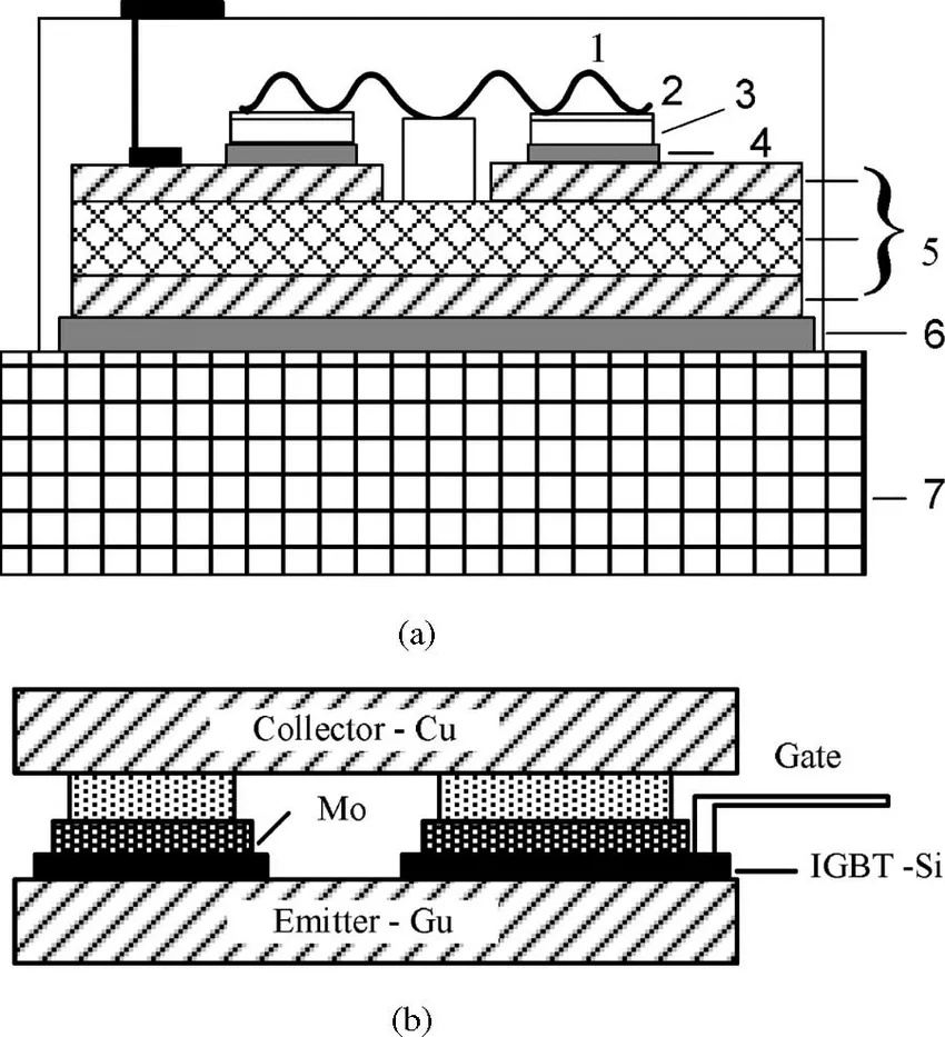
An IGBT module integrates IGBT chips and freewheeling diode (FWD) chips into a modular package using specific circuit interconnections. Packaged IGBT modules are directly used in equipment such as inverters and UPS systems.
Characteristics and Market
IGBT modules offer energy efficiency, convenient installation and maintenance, and stable thermal performance. In practice, the term "IGBT" often refers to the packaged module. With increased focus on energy efficiency and electrification, IGBT modules are widely applied in rail transit, smart grids, aerospace, electric vehicles, and renewable energy systems.
Manufacturing Process and Flow
Typical production steps: screen printing, automatic pick-and-place, vacuum reflow soldering, ultrasonic cleaning, defect inspection (X-ray), automated wire bonding, laser marking, housing molding, potting and curing, terminal forming, and functional testing.
Packaging integrates multiple IGBTs to improve lifetime and reliability while reducing size and improving efficiency. Common module package types include leaded, pin-type, flat-plate, and disc styles; manufacturers use different names and formats. An IGBT module has three key junctions: the aluminum wire bond points on the silicon die, the solder interface between the die and the ceramic insulating substrate, and the solder interface between the ceramic substrate and the copper baseplate. Failures at these junctions typically result from mismatched thermal expansion coefficients and thermally induced material degradation.
Key packaging technologies
- Thermal management design: thermal simulation is used to optimize chip layout and dimensions, enabling higher output power under the same junction-to-case temperature rise.
- Ultrasonic terminal welding: this can directly weld copper pads and copper bond leads, offering a higher melting point and strength compared with conventional soldering and avoiding linear expansion coefficient mismatch.
- High-reliability soldering: conventional Sn-Ag solder can lose strength after thermal cycling, whereas solders such as Sn-Ag-In and Sn-Sb maintain strength under the same cycles, improving high-temperature reliability.
Typical module assembly flow: initial soldering, first wire bonding, secondary soldering, second wire bonding, assembly, housing installation and sealant application, curing, silicone potting, and burn-in screening. Specific steps vary by module; auxiliary steps may include plasma treatment, ultrasonic scanning, testing, and marking.
Functions of Module Packaging
Packaging provides electrical isolation and mechanical protection. Key aspects include colloidal isolation to prevent failures during operation, spring-structured electrode designs to relieve stress and reduce substrate cracking during installation, and baseplate design to ensure close contact with the heatsink to improve thermal cycling capability. Baseplate designs often incorporate a midpoint mounting concept to reduce stress under specified assembly conditions. In application, switching turn-on is relatively gentle for the IGBT, while turn-off is more stressful; many failures occur during turn-off when limits are exceeded.
Technical Details in the Packaging Process
Welding quality directly affects thermal conduction. Vacuum soldering is used for attaching chips to DBC substrates to minimize voids; lower void rates reduce thermal accumulation and the risk of module failure.
Wire bonding provides electrical connections and affects current distribution. In high-current applications (for example, 600 A and 1200 A), bond length and bond placement are critical. Improper bond geometry can cause uneven current distribution and increase the risk of failure. Housing selection requires materials with high temperature resistance, low deformation, moisture resistance, and corrosion resistance to maintain insulation and mechanical protection.
Summary
IGBT module packaging is a complex, precise process involving multiple technical domains, including thermal design, soldering, bonding, and mechanical assembly. Ongoing advances in packaging technologies continue to improve module performance and reliability to meet evolving application requirements.


