 ALLPCB


Calculating PCB dimensions based on component size and placement is a crucial step in PCB layout planning. To determine the right board size, start by listing all components and their footprints, including dimensions and spacing needs. Add extra space for traces, vias, and mounting holes, while considering manufacturing constraints. Use PCB design software to simulate layouts and optimize space. This ensures functionality, manufacturability, and cost-efficiency. In this guide, we’ll dive deep into PCB size calculation methods, component spacing requirements, and practical tips for creating an effective design.
Why PCB Dimensions Matter in Design
Getting the dimensions of a printed circuit board (PCB) right is essential for a successful design. A board that’s too small can lead to cramped components, causing heat issues or signal interference. On the other hand, a board that’s too large wastes material and increases costs. Proper PCB layout planning based on component size and placement ensures that your design works as intended while meeting manufacturing and enclosure requirements.
Beyond functionality, the size of a PCB impacts production costs. Larger boards use more raw materials and may require specialized manufacturing processes. By calculating dimensions accurately, you can balance performance with affordability. Let’s explore how to approach this process step by step.
Step 1: Understand Component Footprints and Sizes
The foundation of PCB size calculation methods lies in understanding the PCB component footprint. A footprint is the physical layout of a component on the board, including its pads, pins, and overall dimensions. Every component—resistors, capacitors, ICs, connectors—has a specific footprint that dictates the space it occupies.
Start by creating a detailed list of all components in your design. For each component, note its dimensions (length, width, and height) and the space needed around it for soldering and heat dissipation. For example, a standard 0805 surface-mount resistor typically measures 2.0 mm x 1.25 mm, while a through-hole connector might need a footprint of 10 mm x 5 mm plus additional clearance.
Many PCB design software tools provide libraries with pre-defined footprints, making this step easier. However, always double-check the datasheet for each component to confirm its exact measurements. Missing even a small detail can throw off your entire layout.
Step 2: Account for Component Spacing Requirements
Once you know the size of each component, the next step is to consider component spacing requirements. Spacing isn’t just about fitting parts on the board—it’s about ensuring reliability and manufacturability. Components placed too closely can lead to soldering issues, overheating, or electromagnetic interference (EMI).
General spacing guidelines include:
- Surface-Mount Devices (SMDs): Maintain at least 0.2 mm to 0.5 mm between components for soldering accuracy.
- Through-Hole Components: Allow 1 mm to 2 mm of clearance to avoid mechanical stress during assembly.
- High-Voltage Areas: Follow standards like IPC-2221, which recommends clearances of 0.6 mm or more for voltages up to 100V to prevent arcing.
- Heat-Sensitive Parts: Place components like power transistors at least 3 mm away from other parts to manage heat dissipation.
Spacing also depends on the manufacturing process. Automated assembly lines often require minimum clearances for pick-and-place machines. Check with your manufacturer for specific guidelines to avoid costly redesigns.
Step 3: Plan for Traces, Vias, and Additional Features
Beyond components, a PCB layout must accommodate traces (conductive paths), vias (connections between layers), mounting holes, and edge clearances. These elements add to the overall dimensions of the board and must be factored into your calculations.
For traces, consider the current they’ll carry. A trace for a low-power signal might be as narrow as 0.2 mm, while a high-current path could require 1 mm or more. Use trace width calculators available in most PCB design software to determine the right size based on current and temperature rise (typically aiming for a rise of no more than 10°C).
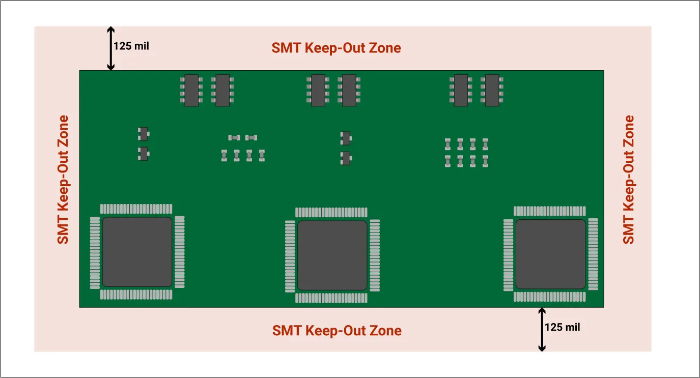
Vias also take up space. A standard via might have a diameter of 0.3 mm with a 0.6 mm pad, so account for these in crowded areas. Mounting holes, often 3 mm in diameter, need clearance around them to avoid interfering with traces or components. Finally, most manufacturers require a 2 mm to 3 mm edge clearance on all sides of the board for handling during production.
Add up these requirements to get a rough estimate of the additional space needed beyond component footprints. This step is critical in PCB layout planning to avoid underestimating the board size.
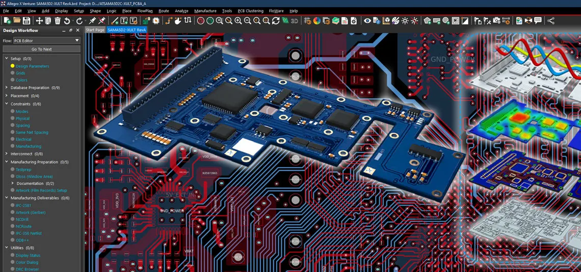
Step 4: Use PCB Design Software for Layout Simulation
Modern PCB design software is a powerful tool for calculating dimensions and testing layouts. These tools allow you to import component footprints, place them on a virtual board, and adjust spacing and routing. They often include design rule checks (DRC) to flag issues like insufficient clearance or overlapping traces.
Here’s a quick PCB design software tutorial for beginners:
- Create a Schematic: Start by designing the circuit schematic, linking components logically.
- Import to Layout Editor: Transfer the schematic to the layout editor, where footprints are assigned to each component.
- Set Board Outline: Define an initial board size based on your rough calculations.
- Place Components: Arrange components, prioritizing critical parts like connectors and power ICs. Group related components (e.g., decoupling capacitors near ICs) to minimize trace length.
- Run DRC: Use the software’s design rule check to ensure spacing and other rules are met.
- Adjust Dimensions: If the layout doesn’t fit, resize the board outline and recheck.
By simulating the layout, you can refine the dimensions before finalizing the design. This iterative process saves time and reduces errors.
Step 5: Consider Enclosure and Mechanical Constraints
The PCB must fit into its intended enclosure or device. During PCB layout planning, check the enclosure’s internal dimensions and account for mounting points, standoffs, and connectors that protrude beyond the board edge. For instance, a USB connector might extend 5 mm past the board, requiring extra space in the enclosure.
Also, consider mechanical stress. If the board will be subject to vibration or flexing, avoid placing heavy components near edges where they could break off. Leave room for screws or clips, typically requiring a 5 mm clearance around mounting holes.
Work closely with mechanical engineers if possible to ensure the PCB dimensions align with the product design. A board that’s even 1 mm too large might not fit, leading to costly delays.
Step 6: Optimize for Manufacturing and Cost
Manufacturing constraints play a big role in finalizing PCB dimensions. Most manufacturers have standard panel sizes (e.g., 18 x 24 inches) from which they cut individual boards. Designing a PCB that fits efficiently into these panels reduces waste and lowers costs.
Additionally, larger boards may require more complex processes, increasing production time and expense. Aim to keep the board as small as possible without compromising functionality. For example, if your initial layout results in a 100 mm x 80 mm board but trimming it to 90 mm x 70 mm still works, you could save on material costs.
Always review the manufacturer’s design guidelines for minimum and maximum board sizes, as well as any specific requirements for edge clearances or panelization. This ensures your PCB size calculation methods align with real-world production capabilities.
Practical Example: Calculating Dimensions for a Simple PCB
Let’s walk through a basic example to illustrate these steps. Imagine designing a PCB for a small IoT device with a microcontroller (10 mm x 10 mm footprint), two sensors (5 mm x 5 mm each), a power connector (8 mm x 3 mm), and 10 passive components (2 mm x 1 mm each).
Step 1: List Component Footprints
- Microcontroller: 10 mm x 10 mm
- Sensors: 2 x (5 mm x 5 mm) = 10 mm x 5 mm total area (approximate)
- Power Connector: 8 mm x 3 mm
- Passives: 10 x (2 mm x 1 mm) = 20 mm x 1 mm total area (approximate)
Step 2: Add Spacing
Assume 1 mm spacing between components. For the microcontroller and sensors, add 1 mm on each side where they’re adjacent. This increases the effective area slightly.
Step 3: Estimate Layout Area
Arranging components in a rough grid, the microcontroller and sensors might fit in a 20 mm x 15 mm block. Passives can be placed around them, adding another 5 mm in one direction. The connector goes on the edge, extending the length by 8 mm. Initial estimate: 25 mm x 20 mm.
Step 4: Add Traces and Edge Clearance
Allow 5 mm total for traces and vias, plus 2 mm edge clearance on all sides. New estimate: 29 mm x 24 mm.
Step 5: Simulate in Software
Using design software, place components and route traces. If everything fits within 30 mm x 25 mm with no DRC errors, finalize at this size.
This example shows how each factor builds on the last to arrive at a practical board size.
Tips for Accurate PCB Size Calculation
Here are some additional pointers to refine your PCB size calculation methods:
- Start with Critical Components: Place connectors, large ICs, or power components first, as they often dictate layout and board edges.
- Group by Function: Keep analog and digital sections separate to reduce noise, even if it slightly increases board size.
- Plan for Future Changes: Leave 10-15% extra space for unexpected additions or revisions.
- Use Standard Sizes: If possible, match dimensions to common enclosure sizes or panel layouts to save on costs.
Common Mistakes to Avoid in PCB Layout Planning
Even experienced designers can make errors in PCB layout planning. Watch out for these pitfalls:
- Ignoring Height: Tall components like electrolytic capacitors can interfere with enclosures if not considered.
- Underestimating Trace Space: Crowded traces can lead to signal crosstalk, especially in high-speed designs where impedance might be 50 ohms or less.
- Forgetting Thermal Management: Place heat-generating parts near board edges or add copper pours for heat sinking, which may require extra space.
- Skipping DRC: Always run a design rule check in your software to catch spacing or clearance issues early.
Conclusion: Mastering PCB Dimensions for Better Designs
Calculating PCB dimensions based on component size and placement is a blend of science and strategy. By understanding PCB component footprints, adhering to component spacing requirements, and leveraging PCB design software, you can create boards that are functional, manufacturable, and cost-effective. Whether you’re a beginner or a seasoned engineer, following structured PCB size calculation methods ensures your designs meet both technical and practical needs.
Take the time to plan your layout carefully, simulate it with software, and consult manufacturing guidelines. A well-sized PCB not only performs better but also saves you from costly redesigns down the line. With these steps and tips, you’re well-equipped to tackle your next project with confidence.


