ALLPCB


In the fast-paced world of electronics, High-Density Interconnect (HDI) PCBs are at the forefront of innovation, enabling smaller, faster, and more powerful devices. However, the HDI PCB assembly process comes with unique challenges, from intricate soldering to precise component placement. In this comprehensive guide, we’ll explore the hurdles of HDI PCB assembly and share best practices to overcome them, focusing on key areas like soldering challenges and component placement techniques. Whether you’re an engineer or a manufacturer, this blog will provide actionable insights to streamline your HDI PCB projects.
What is HDI PCB Assembly?
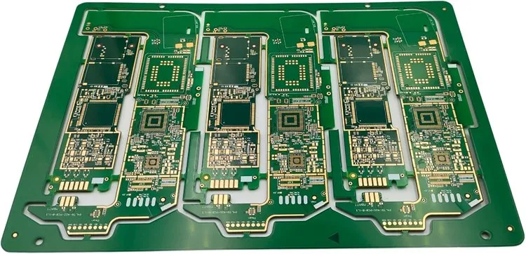
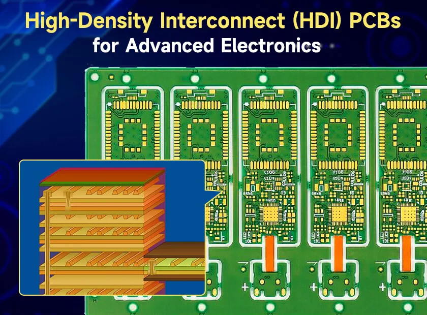
HDI PCB assembly refers to the process of manufacturing and assembling printed circuit boards with a higher wiring density per unit area compared to traditional PCBs. These boards use advanced technologies like microvias, blind and buried vias, and finer traces to pack more functionality into a smaller space. HDI PCBs are essential for modern devices such as smartphones, wearables, and medical equipment, where size and performance are critical.
While the benefits of HDI PCBs are clear—reduced size, improved signal integrity, and enhanced performance—the assembly process is complex. Let’s dive into the specific challenges and best practices to ensure success in the HDI PCB assembly process.
Key Challenges in the HDI PCB Assembly Process
The HDI PCB assembly process is intricate due to the compact design and advanced technologies involved. Below are some of the most common challenges faced during assembly.
1. Miniaturization and Component Density
One of the primary challenges in HDI PCB assembly is the sheer density of components on the board. With trace widths often as narrow as 3 mils (0.003 inches) and spacing equally tight, there’s little room for error. This miniaturization leads to difficulties in placing components accurately and ensuring they function without interference.
Additionally, the use of microvias—tiny holes with diameters as small as 0.006 inches (150 micrometers)—complicates the drilling and plating processes. Any misalignment or defect can lead to signal loss or board failure.
2. HDI PCB Soldering Challenges
Soldering on HDI PCBs is particularly tricky due to the small pad sizes and tight spacing. Components like Ball Grid Arrays (BGAs) and Quad Flat No-leads (QFNs) are common in HDI designs, but their fine-pitch leads (sometimes as close as 0.4 mm) make soldering prone to issues like bridging or insufficient solder joints.
Thermal management during soldering is another hurdle. HDI PCBs often have multiple layers (sometimes 8 or more), which can lead to uneven heat distribution. This increases the risk of cold solder joints or component damage due to overheating.
3. HDI PCB Component Placement Precision
Accurate component placement is critical in HDI PCB assembly. With components packed closely together, even a slight misalignment can cause short circuits or connectivity issues. Automated pick-and-place machines must be calibrated to handle tolerances as tight as ±0.001 inches (±25 micrometers) to ensure precision.
Moreover, the use of smaller components, such as 0201 or 01005 packages, adds to the complexity. These tiny parts are harder to handle and more susceptible to defects like tombstoning, where one end of the component lifts off the pad during reflow soldering.
4. Signal Integrity and Crosstalk
Due to the high density of traces and vias, HDI PCBs are prone to signal integrity issues. Crosstalk, where signals from adjacent traces interfere with each other, can degrade performance, especially in high-speed applications where signal speeds exceed 1 GHz. Maintaining impedance control, often within ±10% of the target value (e.g., 50 ohms for many high-speed designs), is essential but challenging.
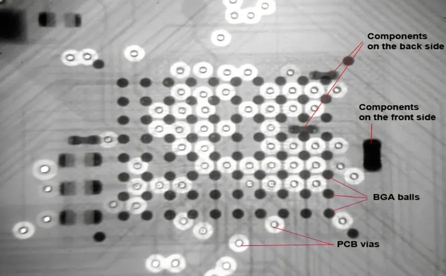
5. Manufacturing and Inspection Limitations
The complexity of HDI PCBs makes inspection and quality control more difficult. Traditional testing methods may not detect defects in microvias or buried layers. Advanced techniques like X-ray inspection are often required, which can increase production costs and time.
Best Practices for HDI PCB Assembly
Despite the challenges, following best practices can significantly improve the success rate of HDI PCB assembly. These strategies focus on precision, process control, and design optimization to address issues like soldering challenges and component placement.
1. Optimize Design for Manufacturability (DFM)
Start with a design that considers manufacturing limitations. Use design software to simulate the layout and identify potential issues before production. Key DFM tips for HDI PCBs include:
- Keep trace widths and spacing within manufacturable limits (e.g., minimum 3 mils for traces and spacing).
- Avoid placing microvias too close to each other to prevent structural weaknesses.
- Ensure sufficient pad sizes for soldering, especially for fine-pitch components.
Collaboration between designers and manufacturers during the early stages can help catch issues before they become costly problems.
2. Use Advanced Soldering Techniques for HDI PCB Soldering Challenges
To tackle HDI PCB soldering challenges, adopt precise soldering methods tailored for high-density boards:
- Reflow Soldering Profiles: Develop a customized reflow profile to ensure even heating across the board. For multilayer HDI PCBs, preheat the board to 150-180°C before reaching peak temperatures of 235-245°C to avoid thermal shock.
- Solder Paste Selection: Use Type 4 or Type 5 solder paste with smaller particle sizes for fine-pitch components to prevent bridging.
- Vapor Phase Soldering: Consider vapor phase soldering for better heat distribution, especially for boards with BGAs or dense component areas.
Regular maintenance of soldering equipment is also crucial to ensure consistent performance and avoid defects.
3. Enhance HDI PCB Component Placement Accuracy
Precision in HDI PCB component placement starts with the right tools and processes:
- High-Precision Equipment: Use advanced pick-and-place machines with vision systems capable of handling components as small as 01005 packages.
- Fixture Support: Employ custom fixtures to hold the PCB steady during placement, minimizing vibrations or shifts.
- Automated Optical Inspection (AOI): Integrate AOI after placement to detect misaligned components before soldering, reducing rework costs.
Training operators to handle miniature components and regularly calibrating machines can further improve placement accuracy.
4. Ensure Signal Integrity in High-Speed Designs
Maintaining signal integrity in HDI PCBs requires careful planning:
- Controlled Impedance: Design traces to match the target impedance, such as 50 ohms for high-speed signals, and use simulation tools to verify performance.
- Minimize Crosstalk: Space high-speed traces apart or use ground planes to shield signals. Keep trace lengths short to reduce signal delay.
- Via Optimization: Use back-drilling to remove unused via stubs that can cause signal reflections in high-speed designs.
Testing signal integrity with tools like Time-Domain Reflectometry (TDR) during prototyping can help identify and fix issues early.
5. Invest in Advanced Inspection and Testing
Quality control is non-negotiable in HDI PCB assembly. Implement the following inspection methods:
- X-Ray Inspection: Use X-ray systems to check for voids or defects in microvias and buried layers.
- Microsectioning: Perform destructive testing on sample boards to analyze via plating quality and layer alignment.
- Electrical Testing: Conduct in-circuit testing (ICT) to verify connectivity and functionality, especially for high-density areas.
These methods, though time-intensive, ensure reliability in the final product, which is critical for applications like medical or automotive electronics.
6. Partner with Experienced Manufacturers
Working with a manufacturer experienced in HDI PCB assembly can make a significant difference. Look for partners with expertise in handling microvias, fine-pitch soldering, and multilayer designs. Clear communication about design requirements and regular feedback during production can prevent misunderstandings and ensure high-quality output.
Benefits of Mastering HDI PCB Assembly
Overcoming the challenges of HDI PCB assembly brings several advantages. Properly assembled HDI PCBs offer improved electrical performance with shorter signal paths, reducing latency in high-speed applications. They also enable compact designs, allowing for innovative products that meet consumer demands for smaller devices. Finally, with optimized processes, manufacturers can reduce defects and rework, saving time and costs in the long run.
Conclusion
HDI PCB assembly is a complex but essential process for modern electronics. While challenges like soldering difficulties, component placement precision, and signal integrity issues can pose hurdles, adopting best practices can lead to successful outcomes. By focusing on design optimization, advanced soldering techniques, precise placement, and thorough inspection, manufacturers can navigate the intricacies of the HDI PCB assembly process with confidence.
At ALLPCB, we’re committed to supporting your HDI PCB projects with cutting-edge solutions and expert guidance. Whether you’re tackling soldering challenges or refining component placement, our team is here to help you achieve reliable, high-performance results. Start your next project with the right strategies and tools to bring your innovative designs to life.