ALLPCB


Overview
Static electricity cannot be eliminated, only controlled.
Basic methods to control ESD:
- Block: Provide electrostatic protection by design. Use insulating materials to seal the PCB inside the enclosure so that accumulated charge cannot be released onto the PCB.
- Conduct: If ESD occurs, quickly route the charge to the PCB main GND to dissipate some of the energy.
Common ESD sequence and coupling paths
- When ESD discharges to the enclosure, a voltage V will be established on the enclosure if there is no ideal ground.
- If the system GND is isolated from the enclosure and the internal circuitry is not designed to connect to the enclosure, the main interference path into internal circuits is coupling.
- If coupling dominates the interference, various mitigations are possible.
- Some portion of the interference will couple into internal circuitry; system grounding is the key to handling these coupled disturbances.
- Air discharge is mainly radiative in the near field and has no clearly defined conduction path. For capacitive coupling, the disturbed area may be large and close, making paths difficult to identify.
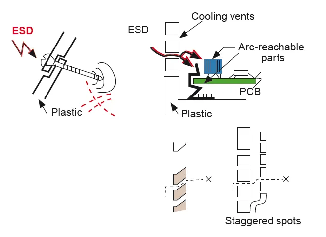
When contact discharge to the metal enclosure occurs, air discharge through gaps must also be considered. Possible symptoms include display flicker, false key inputs, and unexpected resets.
First eliminate direct spark penetration into the electronics. That failure mechanism is direct and easier to identify. The mitigation is to prevent sparks from bypassing the enclosure.
Typical mitigation: reduce mechanical gaps and control internal clearance distances.
Difference between contact and air discharge to the enclosure
Contact discharge on a metal enclosure generates relatively large di/dt. If structural grounding is good, dv/dt is usually small.
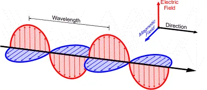
Air discharge to the metal enclosure introduces a large dv/dt at the discharge tip. The larger the high-voltage region at the discharge source, the stronger the dv/dt; this dv/dt can exceed the voltage V generated by contact discharge on poorly grounded metal parts. The spark also produces significant di/dt, creating abrupt electric and magnetic fields.
The abrupt electric field couples capacitively in the near field through insulating parts into internal circuits. The abrupt magnetic field couples inductively through insulating parts into internal circuits.
Recommended three-step approach
A practical approach for system-level ESD design is:
- Prevent external charge from flowing into the PCB and producing transient coupled disturbances.
- Prevent external magnetic fields from producing transient coupled disturbances on the PCB.
- Prevent transient coupling caused by electrostatic fields.
Mitigation options when ESD problems occur
- Improve system grounding design, including chassis, panels, and communication cable terminations.
- Improve PCB grounding design and the ESD grounding for external interfaces.
- Identify root causes of system crashes, resets, or communication errors. Implement signal-level fixes on the PCB and software mitigations where appropriate. These fixes are often the most effective and lowest cost, but can be time-consuming and technically challenging.
Practical recommendations for enclosure and system-level block-and-conduct measures
- Enclosure and structural materials: metals and conductive platings attract and accumulate static. For projects with high ESD requirements, avoid these materials where possible.
- If conductive materials are required: provide effective and evenly distributed grounding points in the structure. In general, pogo pins or metal spring clips provide more reliable grounding than conductive foam or conductive fabric.
- For parts that cannot be grounded, such as plated side keys, apply special handling on the mainboard to mitigate risk.
- Metal parts on the enclosure should be kept at least 2.2 mm away from components and traces.
- Avoid leaving components exposed at holes or gap edges in stacked assemblies. If exposure is unavoidable, use assembly-level measures to block coupling, such as high-temperature tape or anti-static tape. Design mechanical space to allow insertion of isolation pieces where needed.