ALLPCB


1. Why perform EMC design for products?
Answer: To meet functional requirements, reduce debug time, comply with EMC standards, and prevent the product from causing electromagnetic interference to other devices in the system.
2. What aspects should EMC design cover?
Answer: Circuit design (including component selection), software design, PCB layout, enclosure shielding, signal and power line filtering, and grounding scheme.
3. Why are decibels (dB) used in EMC?
Answer: The magnitudes and frequency ranges involved are wide, so logarithmic coordinates are more convenient for graphs; the dB is the logarithmic unit.
4. What foundational knowledge is needed to excel at EMC?
Answer: Learn relevant EMC standards such as EN55022 and EN55024 and basic test principles. Understand EMI components like capacitors, ferrite beads, differential and common-mode inductors. At the PCB level, study layout, layer stackups, and the impact of high-speed routing on EMC. Also develop analysis and mitigation skills for real-world EMC problems.
5. What knowledge should a PCB design novice acquire?
Answer: Familiarity with PCB CAD tools, understanding of the product architecture and schematic circuitry (digital and analog), PCB fabrication and process constraints, high-speed signal integrity, EMI/EMS, SI/PI simulation, and RF knowledge if the product involves RF. For safety creepage/clearance, consult standards such as GB 4943 or UL 60950 and relevant tables.
6. Basic principles of EMC design
Answer: Designers must consider EMC alongside functionality. Key points:
- Component selection: out-of-band response and assembly affect EMC performance.
- Prefer low-inductance capacitors for high-frequency filtering; for leaded capacitors, consider lead inductance impact.
- Electrolytic capacitors can exhibit temporary dielectric breakdown; use solid capacitors where large ripple or transients exist.
- Use low-parasitic resistors; chip resistors are suitable at very high frequencies.
- For low-frequency attenuation, multiple smaller inductors in series can outperform a single large inductor due to parasitic capacitance.
- Watch core saturation in ferrite inductors, especially with high-level pulses.
- Prefer shielded relays and bond the shield to ground.
- Use input transformers with good shielding and isolation.
- Power transformers for sensitive circuits should include electrostatic shielding tied to ground.
- Internal interconnects should be shielded where possible to prevent coupling.
- Use connectors with sufficient pins so shields can be tied to their own pins.
7. Square-wave pulse driving inductive sensors
Answer: Perform tests in a shielded environment or at least shield the sensor and front end. Use differential probes or minimize probe ground lead length. Reduce ringing via routing; consider common-mode suppression and use of chokes where needed. Watch for switching power supply noise and avoid power coupling. If allowed, use current-mode sensing to improve speed and reduce noise. Place analog switches after a front-end amplifier if possible. For waveform concerns, consider frequency compensation or lower operating frequency. Ensure anti-aliasing before ADC and apply software filtering to improve stability.
8. GPS interference in PMP devices with built-in antenna
Answer: Add an ESD filter that provides both ESD protection and EMI suppression at the antenna input. Also consider proper shielding and layout to isolate MCU, memory, and oscillators from the GPS front end.
9. Differential pair design questions
Q&A summary:
- 1) Differential signaling is two lines carrying one signal determined by the voltage difference; it applies to both analog and digital signals.
- 2) A differential port is a four-port network with differential and common-mode behavior. Analyze each using differential and common-mode stimulus and measure Vcm = (V1 + V2) / 2 and Vdm = V1 - V2.
- 3) Differential signals are typically generated by differential driver circuits. Differential amplifiers are characterized by common-mode rejection ratio CMRR = Adm / Acm.
10. Power-line EMI at 30-50 MHz for DC permanent-magnet motor speed control
Answer: LC or Pi filters usually perform better than single capacitors or inductors. For motor supply loops with large low-frequency feedback noise, use larger inductance values and multi-stage capacitive filtering. Ensure the filter design accounts for the motor's noise spectrum and transient behavior.
11. Designing a 0-150 MHz, ≥80 dB gain wideband amplifier - EMC considerations
Answer: Pay attention to low-noise design, stable and clean power supply, input/output impedance matching, decoupling at each stage for HF/LF, deep negative feedback to prevent oscillation, and band-pass filter design. Ensure power distribution and ground noise are controlled. For 150 MHz analog bandwidth, address conducted coupling and power-plane radiation; isolate front-end small-signal and reference supplies to reduce noise.
12. EMC for small DC permanent-magnet motors (90W, 110-120V)
Answer: Motor EMC issues arise from back-emf and commutation arcing. Use motor-design optimization tools and electromagnetic simulation to analyze EMI. Improve commutation, insulation, and consider slot/pole changes, shielding, and filtering. Simulations (Maxwell, etc.) can help evaluate radiation.
13. Using impedance boundary or layered RLC boundaries and EM simulators
Answer: Concentrated resistors can be modeled with RLC boundaries; thin-film resistors can be represented by sheet impedance or impedance editors. Co-simulation using circuit tools and EM solvers (ADS with HFSS/EMPro) is feasible for comprehensive analysis.
14. Static discharge test: contact vs air discharge issue causing a 32 kHz oscillator to stop at 8 kV air discharge
Answer: With metal present, air and contact discharge behave similarly. Try insulating the metal bracket with an insulating coating to change discharge behavior.
15. Measuring PCB radiation is difficult; can simulation replace measurement?
Answer: Simulation cannot fully replace measurement. Tools like Ansys SIwave for PCB noise/radiation and HFSS for 3D high-frequency structures can simulate near-field and far-field emissions and shielded environments. Simulation effectiveness depends on problem definition and model setup. Many EMI issues can be analyzed and mitigated via simulation, but validation by measurement is still required.
16. Ansys EMC tools frequency range and interoperability
Answer: Ansys tools can simulate from DC to tens of GHz; they model lossy transmission lines accurately above 1 GHz. ADS/HyperLynx focus on SI and some EMI aspects; they lack PI analysis. EMC issues involve many factors beyond SI, including power-plane noise, decoupling, shielding, and current distribution. Ansys SIwave interfaces with Mentor PADS.
17. When to use split power planes vs. partitioned ground planes
Answer: Ground plane partitioning isolates noisy and sensitive domains, such as digital and analog. Partitioning must be managed to avoid cross-partition signal-integrity issues; simulation tools can assess isolation. Alternatives include layer stacking, decoupling, and single-point connections where appropriate.
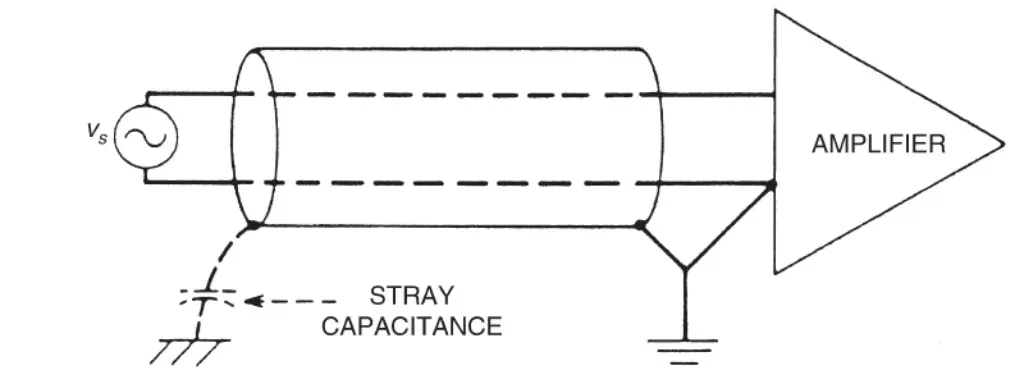
18. Capacitor across two power copper regions used as a high-frequency return path - what passes through the capacitor?
Answer: The capacitor provides a local AC return path; although supply rails are low-pass filtered, switching digital circuits inject AC currents into the power network. The capacitor helps supply instantaneous current to the load and reduces voltage perturbations on the supply by providing a low-impedance local source at high frequencies.
19. Mobile phone fails radiated test at 50-60 MHz, likely charger-related; will adding capacitors at the phone input help?
Answer: Try increasing value of large capacitors and reducing values of smaller ones as needed, and experiment with grounding or shielding the charger inductor enclosure. Tune decoupling and shielding around suspected sources. Testing and targeted mitigation at the phone-side input can be effective without modifying the charger.
20. How to avoid high-frequency interference in PCB design?
Answer: Reduce HF electromagnetic field generation and crosstalk by increasing separation between high-speed and analog signals, using ground guard or shunt traces adjacent to sensitive analog traces, and controlling digital ground noise.
21. Resolving conflicts between high-speed routing and EMI
Answer: Prioritize layout and layer stack techniques (e.g., route high-speed signals on inner layers) to reduce EMI before adding damping components. If filtering or ferrites are used, ensure they do not violate electrical specifications for the signals.
22. How should grounds be connected between multiple PCBs in a system?
Answer: Return currents follow the lowest impedance path, so provide sufficient ground pins at interconnects to reduce impedance and noise. Analyze current loops and guide large currents along controlled paths to minimize impact on sensitive circuits.
23. Can a ground trace be placed between differential pair traces?
Answer: Generally no. Inserting a ground between differential pair traces breaks coupling, harming differential benefits like common-mode noise rejection and flux cancellation.
24. Principles for selecting PCB-to-chassis grounding points
Answer: Choose chassis ground connections to provide low-impedance return paths and to control return current paths. Use nearby screw connections to bond PCB ground to chassis close to high-frequency components or clock sources to minimize loop area and radiation.
25. Techniques for high-speed, high-density PCB design (>100 MHz)
Answer: Control continuous characteristic impedance, maintain sufficient spacing (typically two times line width as a guideline), select appropriate termination, avoid aligned routing on adjacent layers, consider blind/buried vias to save routing area (at higher cost), and provision differential/common-mode terminations to mitigate timing and SI issues.
26. Why can LC filtering perform worse than RC filtering in some cases?
Answer: LC performance depends on targeted frequency band and inductor value. If the noise is at low frequency and the inductance is insufficient, LC may underperform. RC filters dissipate energy and reduce efficiency; resistor power handling must be considered.
27. How to choose inductor and capacitor values for filters?
Answer: Select inductance based on the noise frequency and transient current needs. Large inductance can impede required instantaneous currents, increasing ripple. Capacitor values depend on allowable ripple; ESR and ESL affect performance. For switching regulator outputs, account for filter poles/zeros on feedback loop stability.
28. Balancing EMI and signal integrity in standards and design
Answer: SI and EMC are related but different. To balance both, meet SI requirements while reducing edge rates where possible to lower high-frequency content. Standards typically cover EMC but SI is addressed via design practices rather than mandatory external standards.
29. Achieving EMC on PCB without excessive cost
Answer: Board-level cost drivers include additional plane layers and suppression components. Board techniques to reduce emissions include slowing slew rates, placing HF devices away from external connectors, ensuring impedance matching and consistent return paths, using appropriate decoupling with relevant frequency response, routing connector grounds to chassis locally, and using ground guards cautiously. Also, allow power planes to be inset relative to ground plane by about 20 times the plane separation to reduce common-mode emission.
30. Why separate analog and digital grounds on a mixed-signal PCB?
Answer: Digital switching generates ground and supply noise that can disturb sensitive analog circuits. Separate grounds can be used when analog sections are physically distant from noisy digital sections; otherwise digital noise will couple into analog circuits if grounds are continuous and noisy.
31. EMC/EMI rules to consider in high-speed PCB design
Answer: Consider both radiated (typically >30 MHz) and conducted (<30 MHz) emissions. From the start, plan component placement, stackup, critical interconnect routing, and component choices. Keep clock sources away from connectors, route high-speed signals on inner layers with continuous reference, minimize loop areas, choose decoupling capacitors matching frequency response, use plane partitioning to limit noise spread, and select chassis bonding points appropriately.
32. Use of stackup arrangement to reduce EMI
Answer: Stackup should provide the shortest return paths, minimize coupling area, and suppress differential-mode emissions. Tight coupling between ground and power planes and minor plane insets can help suppress common-mode interference.
33. Why pour copper on PCB?
Answer: Copper pour serves multiple purposes: EMC shielding, PCB manufacturing requirements (plating and lamination), signal integrity by providing continuous return paths, thermal dissipation, and mechanical support for special components.
34. What do FCC and EMC mean?
Answer: FCC is the U.S. Federal Communications Commission, a standards organization. EMC stands for electromagnetic compatibility. Standards and test methods are published to ensure products meet EMC requirements.
35. Should ground traces be arranged in closed loops to reduce interference?
Answer: To minimize interference, reduce loop area. Ground traces should not be routed as closed loops; a tree-like structure with maximized ground area is preferred.
36. How to avoid crosstalk in PCB design?
Answer: Crosstalk occurs during signal transitions. Faster edges produce greater crosstalk. Coupling can be modeled as parasitic capacitance and inductance producing forward and backward crosstalk. Analysis modes include default, tri-state, and worst-case aggregation. Maintain spacing, control impedances, and consider termination and topology to reduce crosstalk.
37. Clock harmonics exceed limits in EMC testing; only decoupling capacitors used on power pins
Answer: Identify the propagation path of the harmonics (radiated vs conducted). Power decoupling addresses conducted paths. Also consider matching, shielding, and controlling return paths. Proper decoupling, routing, and shielding are needed based on the propagation mechanism.
38. Why split grounds into protective and signal grounds or digital and analog power grounds?
Answer: Splitting grounds is an EMC strategy to prevent digital ground and supply noise from coupling to sensitive signals. Protective ground handles ESD/surge considerations. Ultimately there is one earth reference; partitioning controls noise discharge paths.
39. Is it necessary to place ground traces on both sides of a clock trace as shields?
Answer: Adding shield ground traces depends on existing crosstalk/EMI. Improper handling of shield traces can worsen the situation. Evaluate case-by-case.
40. Do near-end and far-end crosstalk depend on signal frequency and rise time?
Answer: Yes. Crosstalk magnitude relates to signal slew rate (V = L * di/dt). Faster transitions cause more coupling. The impact on digital decision levels depends on signal frequency and timing; higher frequencies increase susceptibility.
41. Which PCB stackup is preferred between two presented options?
Answer: Both stackups have merits. Option 1 preserves plane continuity; Option 2 increases the number of ground planes and lowers power-plane impedance, which helps EMI. Practically, ground planes are preferred as the reference for signals. Layer dielectric thickness and plane adjacency affect return completeness across split power planes; ensure signal return continuity across splits.
42. PCB design tips for a system with 89C51 MCU, 12 MHz crystal, ultrasonic and audio signals
Answer: Reduce edge rates where possible and shorten routing. Use matching and topology to control reflections and overshoot. Physically separate noisy and sensitive circuits, route critical signals short, and ensure good grounding and decoupling practices.
43. Should power distribution and routing be treated like ground routing?
Answer: Yes. If power is implemented as a plane, treat it similarly to ground. To reduce common-mode radiation, inset the power plane relative to the ground plane by a factor related to the plane separation. For routed power, avoid closed loops; use tree structures and keep loops small.
44. TFT LCD display susceptible to impulsive EMC causing image wobble
Answer: Standalone LCDs often fail pulse immunity tests. In systems, mitigation includes signal-line decoupling, impedance reduction at the display input using conductive adhesive or shielding the display surface with conductive mesh, and improving the entrance impedance to the LCD signals.
45. Replacing handset casing with ferromagnetic conductive paint removed spurious emissions but introduced new spectral lines around the main frequency
Answer: Verify the handset type, frequency band, and coating material properties (ferromagnetic or conductive, conductivity). Changing the enclosure can alter antenna loading and resonances, causing new emissions or shifting the primary frequency. Characterize coating properties and evaluate enclosure effects on RF performance.
46. Using "pour over all same net objects" in Protel/Altium when copper pouring - any side effects?
Answer: For mixed-signal boards, separate analog, digital, and ground regions then tie at a single point. For high-speed lines, parallel ground traces help. "Pour over all same net objects" does not adversely affect signal performance; it increases pad-to-copper contact area and can help EMI. For wave soldering/reflow, prefer hatched pours around pads to reduce tombstoning risk.
47. What are ferrite beads and when to use inductors or 0-ohm links?
Answer: Ferrite beads suppress high-frequency noise and spikes on signal and power lines, acting as lossy elements at RF while passing DC. Inductors store energy and are used in LC resonant circuits and low-to-mid frequency filters. Choose beads whose impedance peaks in the unwanted noise band and whose low-frequency insertion loss is minimal. Consider DC bias effects and temperature. Use inductors in resonant or low-frequency filtering; ferrite beads for RF noise suppression.
48. How to determine capacitance value to eliminate crosstalk between wires?
Answer: Minimize parallel long traces for high-speed/high-amplitude signals. Where unavoidable, increase spacing, add ground isolation, or use shielding. If area is constrained, use metal shielding or ground planes and consider targeted filtering; exact capacitance selection depends on the coupling frequency range and impedance.
49. Device interference when connecting to automotive chassis ground while paralleling a small auxiliary battery
Answer: Likely automotive EMC interference from sparking or wiring. Key mitigations: review PCB ground routing and copper pours, improve enclosure shielding (metal chassis or conductive tape), separate power and CPU sections, use short, thick power traces, recommend 4-layer boards for automotive use, and try ferrite cores on power leads. Specific fixes vary per system.
50. Why place series resistors on SCL, SDA, and address lines and how to choose values?
Answer: Pull-ups strengthen noise immunity; typical values are VCC/1mA to 10k. Series resistors act as damping; typical values range 33 Ω to 470 Ω. Series resistance controls reflections and can reduce EMI by damping high-frequency edge reflections.
51. Radiated emission high at 200 MHz - how to mitigate; how to select ferrite beads; how to reduce oscillator harmonic emissions?
Answer: If harmonics are from a particular device, shield that device and confirm via test. If shielding reduces emissions, implement a permanent shield with proper grounding. Check exposed transmission lines and bond or shield them. For oscillator harmonics, apply local shielding, filtering, or grounding at transmission line entry points. Bead selection should target the offending frequency range for maximum impedance.
52. Software strategies for EMC compliance in a 2 kW vacuum cleaner controlled by phase-angle SCR (soft start and speed control)
Answer: Hardware and layout are critical; software-only solutions are limited. Coordinate with hardware engineers to reduce EMC—slow ramps and avoiding abrupt switching transitions help, but hardware filtering and snubbing are usually required.
53. DA converter radiation at 166 MHz coupled through supply rails; parallel capacitors do not help
Answer: Check power supply quality and consider a dedicated supply for the DAC. Verify output grounding. Insert a ferrite bead in the output line and consider a bead on the supply to attenuate the 166 MHz component.
54. Multi-channel temperature measurement with K-type thermocouples, using charge-pump supplies and AD620/OP07 amplifiers
Answer: For measurements below 0°C, use +/- supplies rather than single-ended. Clean up supply ripple; add LDOs if necessary. Low-frequency filtering significantly affects results. Place multiplexers before amplification to reduce cost and ensure they support differential inputs. Use thermocouple-specific twisted/shielded cabling. Design input filtering per the amplifier datasheets and consider whether the thermocouple cold junction is grounded or referenced—in many cases a floating or referenced cold junction is used according to system needs.
55. Common EMC issues encountered during certification
Answer: Typical problems are radiated emissions (RE), conducted emissions (CE), and electrostatic discharge (ESD). Communications equipment may also need surge immunity. Medical devices commonly face ESD, EFT (fast transients), conducted susceptibility, and radiated susceptibility. Environmental factors (dry climates, thunder-prone regions) influence ESD and surge requirements.