ALLPCB


Chip design is divided into front-end design and back-end design. Front-end design is also called logic design, and back-end design is also called physical design. With the development of DFT technology, some companies place DFT in front-end, some in back-end, and in some cases DFT is considered a mid-stage activity. There is no strict boundary between front-end and back-end; typically, designs related to process technology are considered back-end design.
The diagram below shows a simplified digital IC design flow:
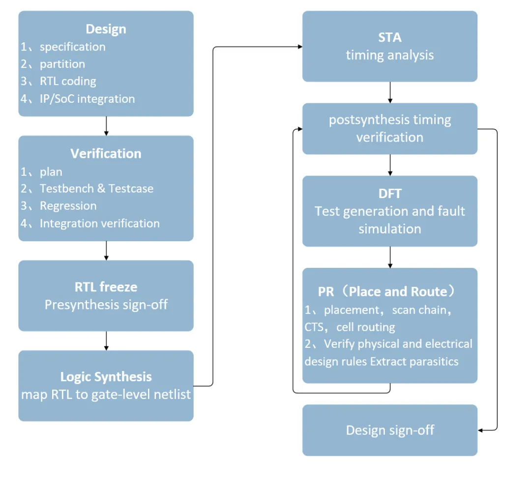
01 Front-end design
1. Requirements analysis
Define the problems the product must solve and forecast trends for the next 3–5 years to ensure the chip has competitive and forward-looking features. Customers provide the fabless design company with functional and performance requirements so architects can refine the specification.
2. Architecture design
Architects decompose system functions and produce a specification, parameterizing and concretizing the design. This includes:
- Processor architecture selection: ARM, RISC-V, etc.
- Bus/interface selection: AHB, AXI, APB, etc.
- Hardware vs. software partitioning: hardware offers higher performance but less flexibility; software offers greater flexibility and shorter development cycles.
- Performance parameters: pinout, voltage and frequency targets, process choice, power, and operating temperature range.
3. RTL coding
Implement module behavior using hardware description languages or graphical entry tools (for example, Cadence Composer).
4. Functional simulation (pre-layout simulation)
Verify RTL code functionality to ensure the design meets the specification. Simulation tools include ModelSim and VCS.
5. Logic synthesis
Using a specific process technology library and target constraints such as area and timing, map RTL to a gate-level netlist. Logic synthesis depends on the chosen synthesis library since standard cell area and timing vary between libraries. A common tool is Synopsys Design Compiler.
6. Static timing analysis (STA)
Verify timing across the circuit and check for setup and hold violations. A common tool is Synopsys PrimeTime.
7. Formal verification
Functionally verify the synthesized netlist by comparing the netlist to the verified HDL to ensure equivalence and that synthesis did not alter the intended circuit behavior. A common tool is Synopsys Formality.
02 Design for Test (DFT, mid-stage)
Design for test (DFT) is an important step in IC design. For logic circuits, scan chains are commonly used to improve controllability and observability of internal states. Scan insertion and optimization are typically performed after logic or physical synthesis. Other DFT techniques include MBIST and ATPG. DFT topics are covered in dedicated articles.
03 Back-end design
1. Placement
Place macrocells and modules on the chip, determining the relative locations of IP blocks, RAM, I/O pins, and so on, which affects final die area. Modern EDA tools widely support physical synthesis, integrating placement optimization with logic synthesis and using real routing information to reduce the number of iterations needed for timing closure. Example tool: IC Compiler.
2. Clock tree synthesis (CTS)
Construct balanced global or local clock distribution trees so that clock arrival time differences to registers are minimized.
3. Routing
Implement the netlist as a physical layout, routing between standard cells and blocks. Routing is typically done in two stages: global routing and detailed routing. After placement, global routing determines placement quality and provides coarse timing estimates. That timing information is back-annotated to the design netlist for STA. Detailed routing proceeds after timing is met, producing accurate timing information.
4. Parasitic extraction
Extract parasitic parameters such as wire resistance and coupling capacitance to analyze signal integrity issues like noise, crosstalk, and reflections.
5. Post-layout simulation
Also called gate-level or timing simulation with back-annotated delays. Use accurate delay values and the post-layout netlist to verify functional and timing correctness. Delays are typically provided via Standard Delay Format (SDF) files.
6. Physical verification
Verify the routed layout for correctness and manufacturability:
- LVS: compare the layout to the synthesized gate-level netlist.
- DRC: design rule checking, e.g., spacing and width rules.
- ERC: electrical rule checking, e.g., shorts and opens.
After completing the above steps, the design can be signed off and delivered to the foundry for tape-out. The back-end flow also includes power analysis. The physical layout is typically delivered in GDS II format to the foundry for wafer fabrication, followed by packaging and testing to produce the final chip.
In practice, different EDA vendors provide toolchains and flows that leverage their tool capabilities, but the overall process is largely consistent. As process nodes shrink, new design flows and EDA tools continue to emerge to address new challenges.