Overview
When designing EMI-resistant circuits and PCB layouts, consider the following aspects:
Key design considerations
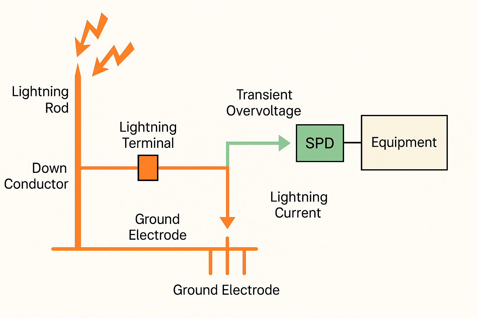
- Use filters: Adding appropriate filters on input and output lines can effectively suppress high-frequency noise and interference signals. Common filters include LC filters, RC filters, and ferrite bead filters.
- Grounding design: Proper grounding is key to reducing EMI. Optimize ground return paths to be as short and direct as possible and avoid ground return loops. Also separate analog and digital grounds to reduce interference between them.
- Good layout planning: Keep sensitive and high-speed signal traces away from noise and radiation sources to reduce mutual interference. Place capacitors and inductors appropriately to lower crosstalk between signal traces.
- Ground isolation: Use separate ground planes or layers to isolate analog and digital circuit grounds, which reduces mutual interference. In PCB design, a layered approach can place analog and digital sections on separate ground layers.
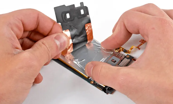
- Shielding and grounding: For sensitive circuits or noise sources, use shields and metal enclosures to block external interference. Proper grounding is essential to ensure effective shielding.
- Component and material selection: Choose components with good EMI performance and prefer low-noise, low-emission devices. For PCB substrates, select materials with low dielectric constant and low loss tangent to reduce energy loss and interference during signal transmission.
EMI testing and certification: standards and methods
EMI testing and certification evaluate the immunity of electronic devices or systems in electromagnetic environments, ensuring compliance with applicable standards and regulations. These tests are usually performed by specialized test laboratories or certification bodies.
The general steps for EMI testing and certification are:
- Determine applicable standards: Identify the international, regional, or industry standards relevant to the product, for example EN55022 in Europe or FCC Part 15 in the US. These standards specify test methods and limits to ensure devices operate properly in electromagnetic environments and minimize interference to other equipment.
- Design-phase testing: Use bench testing and simulation during the product design phase to predict and optimize EMI performance. This helps identify and resolve potential EMI issues before manufacturing.
- Laboratory testing: Submit samples to a certification laboratory for EMI testing. Tests typically include radiated emissions and conducted emissions. Radiated emissions tests evaluate the level of electromagnetic energy radiated into space, and conducted emissions tests measure interference voltages and currents conducted through connection or power lines.
- Test reports and certification application: The laboratory provides a test report that includes results, conformity assessment, and recommendations. Based on the results, decide whether modifications and optimizations are needed. If the product passes the tests and meets the relevant standards, submit a certification application to obtain the corresponding EMI certification or certificate.
Note that specific EMI testing and certification processes may vary by region and product type.
 ALLPCB


