In the intricate world of printed circuit board (PCB) design, achieving reliability and performance often comes down to the smallest details. One such detail, often overlooked, is copper pour balancing. But what exactly is copper pour balancing, and why is it so critical? Simply put, copper pour balancing involves distributing copper evenly across a PCB’s layers to prevent issues like warping, improve mechanical stability, ensure signal integrity, and enhance thermal management. In this comprehensive guide, we’ll dive deep into the benefits of PCB copper balancing, including PCB warping prevention, mechanical stability, signal integrity, and thermal management, to help engineers and designers create more robust and reliable boards.
What Is Copper Pour Balancing in PCB Design?
Copper pour balancing refers to the practice of evenly distributing copper across the layers of a PCB, particularly in areas not occupied by traces or components. This is often achieved by filling unused spaces with copper, also known as copper flooding or copper fill. The goal is to create a uniform copper density across the board to avoid uneven stress during manufacturing and operation. Without balanced copper distribution, a PCB can face a range of problems, from physical deformation to electrical performance issues.
Balancing copper isn’t just about aesthetics; it’s a fundamental aspect of design that impacts the board’s durability and functionality. Whether you’re working on a simple single-layer board or a complex multi-layer design, understanding and implementing copper pour balancing can make a significant difference in the final product.
Why Copper Pour Balancing Matters for PCB Reliability
The importance of copper pour balancing cannot be overstated. It plays a critical role in multiple aspects of PCB performance. Below, we’ll explore how it contributes to warping prevention, mechanical stability, signal integrity, and thermal management—key factors that determine the reliability of any PCB.
1. PCB Warping Prevention: Avoiding Physical Deformation
One of the most immediate benefits of copper pour balancing is PCB warping prevention. Warping occurs when there’s an uneven distribution of materials, especially copper, across the board. During the manufacturing process, particularly during soldering or lamination, uneven copper can cause the board to bend or twist due to thermal expansion and contraction. This physical deformation can lead to misaligned components, broken connections, or even complete board failure.
For example, if one side of a double-sided PCB has significantly more copper than the other, the board may bow during the reflow soldering process as the copper-heavy side expands more than the lighter side. Studies suggest that unbalanced copper can increase the risk of warping by up to 30% in multi-layer boards. By balancing copper pour, designers can minimize these stresses, ensuring the board remains flat and structurally sound.
Technique for Warping Prevention: Use copper thieving, which involves adding small, non-functional copper dots or patterns in areas with low copper density. This helps achieve a uniform copper distribution without interfering with the board’s functionality.
2. Enhancing PCB Mechanical Stability
Mechanical stability is another critical area where copper pour balancing shines. A PCB with uneven copper distribution is more prone to mechanical stress, especially in environments with vibration or physical shock. Uneven copper can create weak points on the board, increasing the likelihood of cracks or delamination over time.
Balanced copper pour acts as a structural reinforcement, distributing stress evenly across the board. This is particularly important for larger PCBs or those used in high-stress applications like automotive or industrial electronics. For instance, a well-balanced board can withstand mechanical stress up to 20% better than an unbalanced one, based on industry testing standards.
Technique for Mechanical Stability: Ensure symmetry in copper distribution not just within a single layer but across all layers of a multi-layer PCB. This can be achieved by mirroring copper patterns on opposing layers to maintain structural balance.
3. Boosting Signal Integrity in High-Speed Designs
Signal integrity is a major concern in modern PCB designs, especially for high-speed applications where even small interferences can cause data errors. Copper pour balancing plays a vital role in maintaining signal integrity by providing a consistent ground plane and reducing electromagnetic interference (EMI).
An unbalanced copper pour can create impedance mismatches, leading to signal reflections and crosstalk. For high-speed signals operating at frequencies above 100 MHz, impedance mismatches as small as 5 ohms can degrade performance. A balanced copper pour, connected to ground, acts as a reference plane, ensuring stable impedance and minimizing noise. This is especially crucial for differential pairs and RF circuits where signal integrity is paramount.
Technique for Signal Integrity: Use via stitching alongside copper pour to connect ground planes across layers. This creates a low-impedance path for return currents, reducing loop inductance and improving signal quality.
4. Improving Thermal Management for Longevity
Thermal management is another area where copper pour balancing offers significant benefits. Copper is an excellent conductor of heat, and a balanced pour can help dissipate heat evenly across the board. Without proper balancing, hotspots can form in areas with high component density or power dissipation, leading to thermal stress and potential component failure.
For example, in power electronics, components like MOSFETs can generate significant heat, sometimes exceeding 100°C. A balanced copper pour can spread this heat, reducing peak temperatures by as much as 15-20°C compared to an unbalanced design. This not only extends the lifespan of components but also prevents thermal-induced warping.
Technique for Thermal Management: Extend copper pour areas near high-power components and connect them to thermal vias. These vias can transfer heat to other layers or a heat sink, improving overall thermal dissipation.
Practical Techniques for Achieving Copper Pour Balancing
Now that we’ve covered the benefits of PCB copper balancing, let’s explore actionable techniques to implement it effectively in your designs. These methods are practical and can be applied using most modern PCB design software.
1. Use Copper Thieving for Uniform Density
Copper thieving involves adding small, non-functional copper shapes or dots in areas with low copper density. This technique is particularly useful during the etching process, as it prevents over-etching in sparse areas and ensures uniform plating. Thieving patterns should be placed at least 0.2 mm away from active traces to avoid interference.
2. Implement Hatch Patterns for Controlled Fill
In some cases, a solid copper pour may not be ideal due to manufacturing constraints or signal integrity concerns. Hatch patterns, which use a grid-like copper fill, offer a middle ground. They provide balanced copper distribution while reducing the risk of floating copper islands that can act as antennas for EMI. A common hatch density is 25-50%, depending on the board’s requirements.
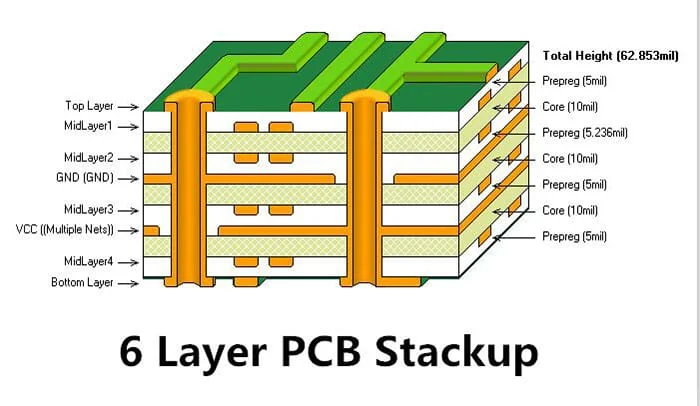
3. Mirror Copper on Multi-Layer Boards
For multi-layer PCBs, ensure that copper distribution is mirrored across corresponding layers. For instance, if layer 1 has a dense copper area, layer 2 should have a similar density in the same region. This symmetry reduces the risk of warping and improves mechanical stability.
4. Connect Copper Pour to Ground or Power Planes
Always connect copper pour to a ground or power plane unless there’s a specific reason not to. This not only improves signal integrity by providing a return path but also aids in thermal management by distributing heat. Ensure proper spacing (typically 0.15-0.3 mm) between the pour and unrelated traces to prevent short circuits.
Common Challenges and How to Overcome Them
While copper pour balancing offers numerous benefits, it’s not without challenges. Here are some common issues and solutions to ensure success.
Challenge 1: Overfilling Leading to EMI Issues
Excessive copper pour, especially if not grounded, can act as an antenna, picking up or radiating EMI. To avoid this, always tie copper pours to ground and use hatch patterns in sensitive areas to minimize parasitic capacitance.
Challenge 2: Manufacturing Constraints
Some manufacturers may have limitations on copper density or thieving patterns due to etching or plating processes. Work closely with your fabrication partner to understand their design rules and adjust your copper pour strategy accordingly.
Challenge 3: Balancing vs. Routing Space
In densely populated boards, finding space for copper pour can be difficult. Prioritize critical areas like ground planes near high-speed signals and use smaller thieving patterns in tight spaces to maintain balance without sacrificing routing area.
Conclusion: Make Copper Pour Balancing a Priority
Copper pour balancing may not be the most glamorous aspect of PCB design, but it’s undoubtedly one of the most impactful. From PCB warping prevention to enhancing mechanical stability, ensuring signal integrity, and optimizing thermal management, the benefits of PCB copper balancing are clear. By implementing techniques like copper thieving, hatch patterns, and symmetric layering, designers can create boards that are not only reliable but also perform at their best under demanding conditions.
Whether you’re designing a simple prototype or a complex multi-layer board, don’t overlook the power of balanced copper distribution. It’s the unsung hero that can make or break your PCB’s reliability. Take the time to integrate these practices into your workflow, and you’ll see the difference in the quality and longevity of your designs.
 ALLPCB


