ALLPCB


Common ESD protection devices include diode, resistor, P/NMOS, BJT, and SCR. Because these devices can enter a low-resistance state instantly via mechanisms such as avalanche breakdown and avalanche injection, they have good ESD current-sinking capability and are used as ESD protection elements.
1. Diode
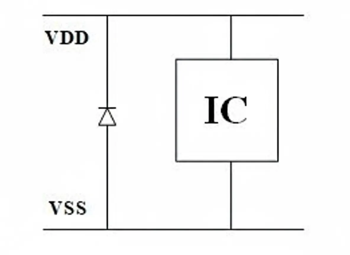
Diodes are commonly used for ESD protection. In the typical application, when VDD is driven positive relative to VSS by an ESD pulse, the diode avalanches and discharges the ESD current, protecting internal circuitry. Because the diode discharges ESD energy mainly by avalanche breakdown, device power dissipation can be large under high currents; therefore, reverse-breakdown diodes often have relatively low ESD robustness and higher differential resistance. Conversely, when VDD is negative relative to VSS, the diode is forward biased and conducts the ESD current. The forward conduction voltage is small, so power dissipation is low and the diode shows strong ESD capability in this mode.
2. MOS & BJT
MOS and BJT devices use a similar ESD discharge mechanism: the parasitic BJT is activated to release the ESD current. Because CMOS processes are widely used, MOS devices are the most common ESD protection elements. To prevent the ESD device from conducting during normal operation, MOS gates are tied so they remain off: gate-grounded NMOS (GG-NMOS) and gate-VDD PMOS (GD-PMOS).
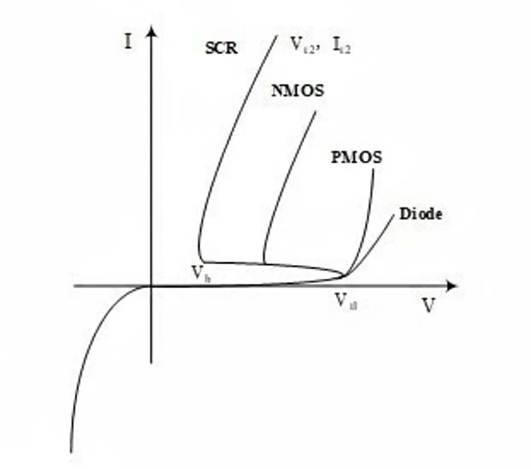
When the drain is driven positive relative to the source by an ESD pulse, the drain N+/Pwell junction avalanches. The hole current produced by the avalanche flows through the Pwell to the P+, producing a voltage drop across the Pwell equivalent resistance Rpw. When this drop exceeds the base-emitter forward voltage of the parasitic NPN device, the parasitic NPN turns on; this trigger voltage is Vt1. After triggering, the parasitic NPN and its amplification mean the device can sustain large current at a relatively low drain voltage, producing snapback and negative differential resistance: over a current range the device voltage decreases as current increases.
As current further increases, the voltage cannot drop indefinitely and parasitic resistances take effect, so the negative resistance region transitions to positive resistance. The minimum voltage during this transition is the hold voltage Vh, which characterizes the lowest clamping voltage the device can provide. At very high currents, heat-induced carrier generation inside the device can dominate avalanche/injection carriers, and higher temperature increases thermally generated carriers, forming positive feedback. This produces a secondary snapback associated with thermal breakdown; the voltage and current at that point are the secondary breakdown voltage Vt2 and current It2, which indicate device destruction conditions and maximum survivable current. Ultimately, excessive temperature leads to permanent device damage. For a negative ESD pulse at the drain relative to source, the current can be discharged through the forward-biased source P+/Pwell/N+ diode.
Compared with NMOS, PMOS uses the parasitic PNP BJT for current discharge, whose current gain is much lower than the parasitic NPN in NMOS. Therefore, PMOS devices may not exhibit snapback and are generally less effective for ESD protection; PMOS is typically used only between VDD and I/O pins.
3. Resistor
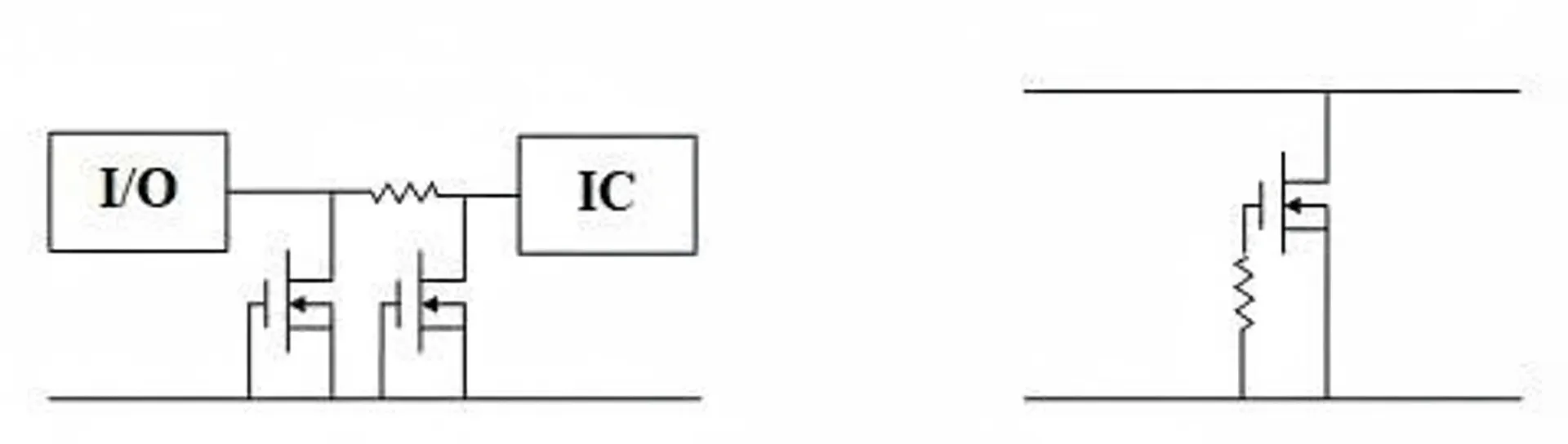
Resistors are not used alone for on-chip ESD protection; they are used as auxiliary elements, for example as a series resistor between the first and second stages of input protection. When the ESD current is too large and the first-stage device cannot clamp the voltage to a safe region, conduction of the second-stage device forms a voltage divider with the resistor, further reducing the voltage reaching internal circuits. Another example is the gate resistor in GG-NMOS: the NMOS gate is connected to ground through a resistor rather than directly. During a positive ESD pulse at the drain, drain-to-gate capacitance couples a positive potential to the gate, which helps turn on the NMOS channel and lowers the device trigger voltage under ESD stress.
4. SCR
SCRs provide the strongest ESD protection after forward diodes. When the anode sees a positive ESD pulse, the Nwell/Pwell junction avalanches. The resulting electron and hole currents flow through RNw and Rpw and activate the PNP and NPN devices. P+ injects holes into the anode and N+ injects electrons into the cathode; these injected carriers serve as base currents for the NPN and PNP devices, respectively. The positive feedback turns on both devices and produces strong conductivity modulation in the wells, reducing the voltage drop across the device. SCRs therefore have a low hold voltage, very strong ESD capability, and very small differential resistance. For a negative ESD pulse at the anode, current can be released via the forward-biased cathode P+/anode N+ diode.
Because SCR triggering relies on Nwell and Pwell junction breakdown, the breakdown voltage in standard CMOS is typically tens of volts, much higher than the gate-oxide breakdown voltage, so the native SCR trigger is too high for low-voltage CMOS protection. For low-voltage chips, the SCR trigger voltage must be reduced by design techniques to meet protection requirements.
SCRs have high It2, allowing a small device width to meet on-chip ESD requirements and thereby reduce parasitic capacitance introduced by ESD structures. This is beneficial for RF chip ESD design.
5. Comparative ESD Performance
For common CMOS/BCD processes, whether for low-voltage or high-voltage applications, the per-unit-area ESD protection capability is approximately: SCR > MOS > diode (reverse breakdown).