ALLPCB


Memory area growth in modern CCDs
AMD’s move to advanced process nodes for CCDs has highlighted the cost and area impact of on-chip SRAM. In TSMC 5nm-based Zen 4 CCD layouts, L2 and L3 cache already occupy roughly half of the die area, driving design tradeoffs between core count, memory bandwidth, and on-die cache capacity.
3D V-Cache: stacking SRAM to boost capacity
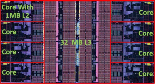
To mitigate memory performance limitations from relatively low per-core memory bandwidth, increased core-to-memory latency, and limited cross-CCD bandwidth, AMD has used larger L3 caches as a compensating mechanism. From Zen 2 to Zen 4, CCD L3 size remained at 32 MB, so AMD separated SRAM scaling from the CPU die itself.
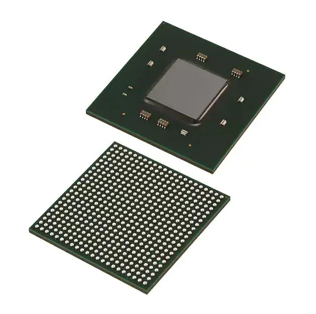
AMD introduced first-generation 3D V-Cache on Milan-X EPYC 7003X processors. These use Zen 3 cores and add an L3 cache die (L3D) of 64 MB manufactured in 7 nm, with each L3D die about 41 mm2. The L3D is vertically bonded to the CCD using hybrid bonding and TSV (through-silicon vias). The stacked assembly includes four parts: the CCD at the bottom, the L3D above it, and supportive silicon structures at the sides to planarize the stack and help conduct heat from the CCX (core complex) up to the package lid.
In Zen 3, the L3 cache is organized into eight slices of 4 MB each; the L3D is also split into eight slices of 8 MB. Each pair of slices is connected by 1024 TSVs, totaling 8192 TSV connections. AMD reported that the added L3 cache increases latency by about four cycles.
The second-generation 3D V-Cache introduced with Zen 4 increased bandwidth from 2 TB/s to 2.5 TB/s while keeping capacity at 64 MB and the process at 7 nm. Die area was reduced to about 36 mm2, mainly through TSV-area optimizations without reducing TSV pitch. Genoa-X EPYC variants based on this second generation were expected in 2023.
Expanding SRAM capacity raises cache hit rates and reduces the performance penalty from DRAM access. AMD’s 3D V-Cache achieves substantial cache capacity increases at a reasonable cost (roughly doubling L3 capacity for a CCD) and yields measurable performance gains. The tradeoffs include constraints on overall package power and achievable core frequencies, so product selection depends on workload characteristics.
Form-factor and compatibility considerations for stacked SRAM
Stacking external SRAM raises compatibility questions. Stacking on top of the processor is the least compatible form factor; side-stacking limits achievable bandwidth; placing SRAM under the processor requires further adoption of 3D packaging and silicon base layers. Putting SRAM beneath CCDs is not currently feasible in AMD’s CCD+IOD tiled packaging and interposer routing approach, so fundamental changes to chip organization would be required for future architectures such as Zen 5 or Zen 6.
For datacenter processors where core count is a primary metric, small L3D sizes are convenient because each L3D measures only a few dozen mm2. Larger high-performance cores occupy far more area, making vertical SRAM stacking less straightforward. Ultimately, suitability depends on the processor’s internal bus and interconnect topology: vertically stacked SRAM—whether serving as L2 or L3—is better suited to cache-centric ring or centralized-bus architectures.
eDRAM and HBM tradeoffs
x86 server CPUs have not generally adopted eDRAM. On-die eDRAM still occupies significant area, is effectively DRAM technology, and has not advanced to sub-10 nm nodes. IBM’s Power10, manufactured on Samsung 7 nm, does not emphasize eDRAM.
Externally, eDRAM is not a widely standardized product, faces limited market scale, higher cost, and constrained performance and capacity.
HBM (High Bandwidth Memory) addresses many of these issues by decoupling memory from the CPU die, using vertical stacking and TSV/interconnects to increase density, and achieving better standardization. HBM trades latency for capacity and bandwidth by sitting closer to the memory tier than an on-die cache, which is an appropriate tradeoff for many high-bandwidth workloads.
Downward approach: base-layer integration
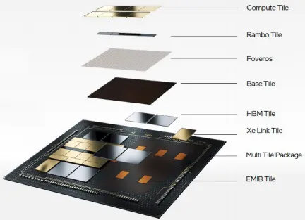
Intel’s data-center Max GPUs introduced the concept of a base tile (base chip). Functionally similar to a silicon interposer but more capable, the base layer can host compute cores, high-speed I/O (including HBM PHYs), and cache. Unlike a simple passive interposer built with mature processes (for example, 65 nm) to provide high-density electrical connections, the base layer can include active logic implemented in more advanced nodes.
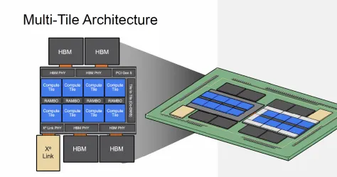
Intel presented a chiplet architecture for the data-center Max GPU in ISSCC 2022. The base chip measures about 640 mm2 and is manufactured on Intel 7. Intel integrated high-speed SerDes and PHYs (HBM PHY, Xe Link PHY, PCIe 5.0) and on-package cache into the base chip, which is similar in role to AMD’s IOD. These circuits are well suited to advanced process nodes, so integrating them in a single base chip is a reasonable packaging choice.
Using Foveros 3D stacking, Intel’s Max GPU stacks eight compute tiles and four RAMBO tiles on top of the base chip. The compute tiles are manufactured in TSMC N5; each compute tile contains private 4 MB of L1. RAMBO tiles (Random Access Memory, Bandwidth Optimized), manufactured on Intel 7, provide cache-like RAM; each RAMBO tile contains four 3.75 MB banks (15 MB per tile). Four RAMBO tiles together provide 60 MB of L3-like capacity. The base chip also contains RAMBO structures totaling 144 MB plus a cache switch fabric.
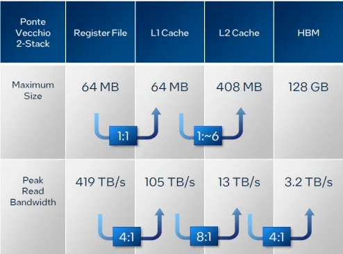
Across the package, the base chip’s cache switch fabric aggregates the 144 MB on-base capacity with the 60 MB from the stacked RAMBO tiles to form 204 MB of L2/L3-equivalent cache per base group; with two such groups in the package, total L2/L3 capacity reaches 408 MB.
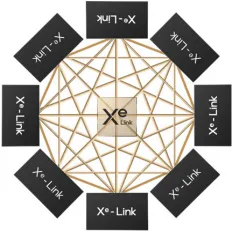
Compute groups connect via Xe Link tiles, which are manufactured on TSMC N7. HBM, Xe Link chips, and neighboring base chips in the same package are connected using EMIB for shorter lateral links and Foveros for vertical stacking.
Intel reported an L2 cache aggregate bandwidth of up to 13 TB/s for the Max GPU. Considering packaging with two base-chip groups, a per-base-group figure of about 6.5 TB/s still far exceeds current Xeon and EPYC L2/L3 cache bandwidths. AMD’s 3D V-Cache already demonstrated that 3D-stacked cache can provide meaningful performance; Intel’s base-chip plus RAMBO approach scales that concept to much larger area budgets.
Thermal and architectural advantages of base-layer cache
One weakness of vertically stacked cache has been thermal dissipation. Integrating large SRAM arrays into a base chip brings thermal benefits: high-power compute tiles are placed above the base chip so heat can be conducted away more effectively. In mesh-based processor architectures, L3 is often partitioned into many units distributed across mesh nodes. A base chip can cover the processor die and partition SRAM into units that map directly to mesh nodes.
For mesh-style processors, moving L3 out to a base chip is therefore a reasonable architectural choice. Current 3D packaging bump pitches in the 30 to 50 micrometer range support hundreds to thousands of connections per mm2, sufficient for current mesh-node bandwidth requirements. Higher-density connections (10 micrometer or submicron) are being developed, but those advances are primarily driven by highly customized internal stacks such as HBM and 3D NAND using hybrid bonding, which may not match Chiplet-level flexibility requirements.