 ALLPCB


When it comes to designing high-performance printed circuit boards (PCBs) with blind and buried vias, the choice of material plays a critical role. While FR-4 has long been the go-to substrate for many PCB applications due to its cost-effectiveness and versatility, it often falls short in high-frequency, high-speed, or high-density designs. For engineers seeking enhanced performance in blind and buried via applications, alternative materials offer superior electrical, thermal, and mechanical properties. In this blog, we’ll dive deep into the world of PCB materials beyond FR-4, focusing on how they improve blind and buried via performance for cutting-edge electronics.
Why Move Beyond FR-4 for Blind and Buried Vias?
FR-4, a composite material made of woven fiberglass and epoxy resin, is widely used for its balance of cost, durability, and performance. However, in high-performance PCB designs—especially those involving blind vias (vias that connect an outer layer to an inner layer without passing through the entire board) and buried vias (vias that connect inner layers without reaching the surface)—FR-4 can present limitations. These include higher dielectric loss, poorer thermal conductivity, and challenges with signal integrity at frequencies above 1 GHz.
Alternative materials address these issues by offering lower dielectric constants (Dk), reduced signal loss, and better thermal management. This makes them ideal for applications like 5G technology, automotive radar, aerospace systems, and high-speed digital circuits. Let’s explore why and how these materials enhance blind and buried via performance.
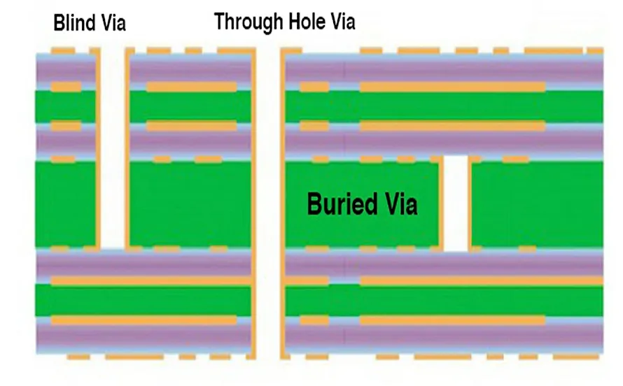
Understanding Blind and Buried Vias in High-Performance PCBs
Blind and buried vias are essential for high-density interconnect (HDI) designs, where space is limited, and multiple layers are needed to route signals efficiently. Blind vias save space by connecting only specific layers without penetrating the entire board, while buried vias remain hidden within internal layers, freeing up surface space for components. These vias are critical for compact, high-performance electronics, but they demand materials that can handle precise drilling, maintain signal integrity, and manage heat dissipation.
Using FR-4 with blind and buried vias can lead to issues like signal degradation due to its higher dielectric constant (typically around 4.2-4.5 at 1 MHz) and dissipation factor (around 0.02). In contrast, advanced materials reduce these values, ensuring cleaner signal transmission and better reliability in complex designs.
Key Challenges with FR-4 in Blind and Buried Via Applications
Before diving into alternative materials, it’s important to understand the specific challenges FR-4 poses in high-performance PCB designs:
- Signal Loss at High Frequencies: FR-4’s higher dielectric loss tangent causes signal attenuation, which is problematic for high-speed data transfer rates above 5 Gbps.
- Thermal Limitations: With a thermal conductivity of about 0.3 W/m·K, FR-4 struggles to dissipate heat in densely packed designs with blind and buried vias.
- Mechanical Issues: The material’s rigidity can lead to cracking or delamination during the precise laser or mechanical drilling required for small-diameter vias.
- Impedance Control: Maintaining consistent impedance in multilayer boards with vias is harder with FR-4 due to variations in its dielectric properties.
These challenges push engineers to explore alternative PCB materials that can meet the demands of modern electronics while supporting intricate via structures.
Alternative PCB Materials for Enhanced Blind and Buried Via Performance
Several high-performance materials stand out as viable alternatives to FR-4, especially for designs requiring blind and buried vias. Below, we’ll explore some of the most effective options, focusing on their properties and benefits.
1. High-Frequency Laminates with Low Dielectric Constants
High-frequency laminates are engineered for applications where signal integrity is paramount, such as in RF (radio frequency) and microwave circuits. These materials typically have a dielectric constant (Dk) ranging from 2.2 to 3.5 and a dissipation factor (Df) as low as 0.001, compared to FR-4’s higher values. This results in lower signal loss and better performance at frequencies up to 10 GHz or more.
For blind and buried vias, these laminates offer improved impedance control and reduced crosstalk, which are critical in HDI designs. They also support finer via structures due to their smoother surface and consistent dielectric properties, making laser drilling more precise.
Key Benefits:
- Signal speeds up to 25 Gbps with minimal loss.
- Stable performance in high-frequency applications like 5G and IoT devices.
- Better compatibility with microvias (vias smaller than 0.15 mm in diameter).
2. Polyimide-Based Materials for Thermal Stability
Polyimide materials are known for their exceptional thermal and mechanical stability, making them ideal for environments with high temperatures or mechanical stress. With a glass transition temperature (Tg) often exceeding 250°C (compared to FR-4’s 130-140°C), polyimide can withstand the heat generated in dense PCB layouts with numerous vias.
In blind and buried via designs, polyimide reduces the risk of delamination or cracking during manufacturing processes like sequential lamination. It also supports reliable performance in aerospace and automotive applications where thermal cycling is common.
Key Benefits:
- Thermal conductivity up to 0.5 W/m·K for better heat dissipation.
- High resistance to thermal expansion, ensuring via integrity.
- Suitable for multilayer boards with up to 20+ layers.
3. PTFE-Based Materials for Ultra-Low Loss
Polytetrafluoroethylene (PTFE) materials, often reinforced with glass or ceramic fillers, are a top choice for ultra-high-frequency applications. With a dielectric constant as low as 2.1 and a dissipation factor below 0.0004, PTFE minimizes signal loss even at frequencies above 20 GHz. This makes it perfect for radar systems, satellite communications, and other cutting-edge technologies.
For blind and buried vias, PTFE materials provide excellent electrical performance and support very small via sizes, down to 0.1 mm or less. However, they can be more challenging to process due to their softness, requiring specialized manufacturing techniques.
Key Benefits:
- Exceptional signal integrity for data rates exceeding 40 Gbps.
- Minimal interference in densely routed designs with multiple vias.
- Low moisture absorption for consistent performance in humid environments.
4. Ceramic-Filled Laminates for High Reliability
Ceramic-filled laminates combine the benefits of low dielectric loss with enhanced mechanical strength and thermal conductivity (up to 1.5 W/m·K). These materials are often used in military and medical devices where reliability is non-negotiable.
In designs with blind and buried vias, ceramic-filled laminates reduce the risk of via failure during thermal stress and support high-density routing with stable electrical properties. They also resist wear during drilling, ensuring precise via placement.
Key Benefits:
- High mechanical strength for reliable via structures in multilayer PCBs.
- Stable dielectric properties across a wide temperature range (-55°C to 125°C).
- Ideal for applications requiring long-term durability.
Comparing Costs and Trade-Offs of Alternative Materials
While alternative materials offer significant advantages over FR-4 for blind and buried via performance, they often come with higher costs and manufacturing complexities. Here’s a quick comparison to help engineers make informed decisions:
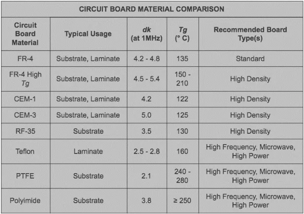
| Material | Dielectric Constant (Dk) | Dissipation Factor (Df) | Thermal Conductivity (W/m·K) | Relative Cost |
|---|---|---|---|---|
| FR-4 | 4.2-4.5 | 0.02 | 0.3 | Low |
| High-Frequency Laminate | 2.2-3.5 | 0.001-0.003 | 0.4-0.6 | Moderate to High |
| Polyimide | 3.4-3.8 | 0.008-0.01 | 0.5 | High |
| PTFE-Based | 2.1-2.5 | 0.0004-0.002 | 0.25-0.5 | Very High |
| Ceramic-Filled Laminate | 3.0-4.0 | 0.002-0.005 | 1.0-1.5 | High to Very High |
Engineers must weigh performance needs against budget constraints. For example, while PTFE-based materials excel in ultra-high-frequency designs, their cost may not be justified for less demanding applications where a high-frequency laminate could suffice.
How to Choose the Right Material for Your Blind and Buried Via Design
Selecting the best material for a PCB with blind and buried vias depends on several factors:
- Frequency and Speed Requirements: For high-frequency or high-speed designs (above 5 GHz or 10 Gbps), prioritize low-loss materials like PTFE or high-frequency laminates.
- Thermal Environment: If the PCB will operate in high-temperature or thermally cyclic conditions, opt for polyimide or ceramic-filled laminates.
- Density and Layer Count: For HDI designs with many layers and microvias, choose materials that support precise drilling and maintain signal integrity.
- Budget Constraints: Balance performance with cost, especially for large-scale production where material expenses can add up quickly.
By carefully evaluating these factors, you can ensure that your PCB design achieves optimal performance without unnecessary costs.
Manufacturing Considerations for Alternative Materials
Switching to alternative materials often requires adjustments in the manufacturing process. For instance, PTFE-based materials may need specialized drilling techniques to avoid deformation, while polyimide requires careful handling to prevent moisture absorption during processing. Working with a manufacturer experienced in handling advanced materials can minimize risks and ensure high-quality results for blind and buried via structures.
Additionally, consider the compatibility of the material with your design software and fabrication processes. Some materials may require specific stack-up configurations or surface finishes to achieve the desired performance.
Future Trends in PCB Materials for Blind and Buried Vias
As technology continues to advance, the demand for even more efficient PCB materials grows. Emerging trends include the development of hybrid laminates that combine the benefits of multiple materials (e.g., low-loss properties with high thermal conductivity) and eco-friendly substrates that reduce environmental impact without sacrificing performance. These innovations promise to further enhance blind and buried via performance in next-generation electronics.
Moreover, advancements in manufacturing techniques, such as additive manufacturing and improved laser drilling, are making it easier to work with advanced materials, potentially lowering costs and expanding their accessibility for a wider range of applications.
Conclusion: Elevating PCB Design with Alternative Materials
While FR-4 remains a reliable choice for many standard PCB applications, it often falls short in high-performance designs requiring blind and buried vias. Alternative materials like high-frequency laminates, polyimide, PTFE-based substrates, and ceramic-filled laminates offer superior electrical, thermal, and mechanical properties, enabling engineers to push the boundaries of PCB design. By understanding the unique benefits and trade-offs of these materials, you can make informed decisions to optimize your next project for signal integrity, thermal management, and overall reliability.
At ALLPCB, we’re committed to supporting your innovation with a wide range of material options and expert manufacturing capabilities. Whether you’re designing for 5G, automotive, or aerospace applications, our team is ready to help you achieve exceptional results with the right materials for your blind and buried via needs.


