ALLPCB


If you're new to RF PCB design and looking for a comprehensive guide to get started, you've come to the right place. This beginner's guide to RF PCB design will walk you through the basics, from understanding key concepts to applying practical techniques. Whether you're searching for an RF PCB design tutorial, RF PCB design basics, or an RF PCB design course, this post covers everything you need to know about RF PCB design for beginners, including tips for learning RF PCB design online.
In the sections below, we'll break down the theory behind radio frequency (RF) circuits, explore essential design principles, and provide actionable steps to create your first RF PCB layout. Let’s dive into the world of high-frequency electronics and build a strong foundation for your projects.
What Is RF PCB Design and Why Is It Important?
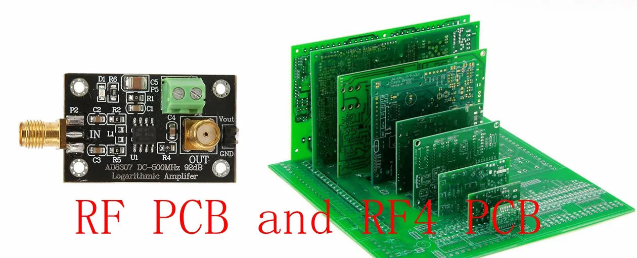
RF PCB design refers to the process of creating printed circuit boards (PCBs) that handle radio frequency signals, typically in the range of 3 kHz to 300 GHz. These boards are used in applications like wireless communication, radar systems, GPS devices, and more. Unlike standard PCB design, RF PCB design requires special attention to signal integrity, impedance matching, and electromagnetic interference (EMI) because of the high-frequency nature of the signals.
The importance of RF PCB design lies in its impact on performance. A poorly designed RF PCB can lead to signal loss, noise, or complete failure of the device. For beginners, mastering RF PCB design basics ensures that your circuits function reliably in real-world applications, whether you're building a simple radio or a complex IoT device.
Key Challenges in RF PCB Design for Beginners
Before we dive deeper, let’s highlight some common challenges in RF PCB design:
- Signal Integrity: High-frequency signals are prone to distortion and loss if traces aren’t designed properly.
- Impedance Matching: Mismatched impedance can reflect signals back, causing inefficiency. For example, a common target impedance for RF traces is 50 ohms.
- EMI and Noise: RF circuits are sensitive to interference from nearby components or external sources.
- Material Selection: Standard PCB materials may not handle high frequencies well, often requiring specialized substrates like Rogers or Teflon.
Understanding the Theory Behind RF PCB Design
To excel in RF PCB design, you must first grasp the fundamental theories that govern high-frequency circuits. This section serves as an RF PCB design tutorial for beginners, breaking down complex concepts into simple terms.
1. What Are Radio Frequency Signals?
RF signals are electromagnetic waves that oscillate at high frequencies. Unlike low-frequency signals, RF signals behave more like waves than direct currents, meaning they can radiate energy and interfere with other signals. This wave-like behavior is why RF PCB design focuses heavily on trace length, width, and spacing to avoid signal reflection and loss.
2. Importance of Impedance Matching
Impedance is the resistance to the flow of an alternating current in a circuit. In RF design, matching the impedance of the source, transmission line, and load (often 50 ohms) is critical to maximize power transfer and minimize signal reflection. For instance, a mismatched impedance can result in a standing wave ratio (SWR) greater than 1:1, leading to power loss.
3. Signal Propagation and Skin Effect
At high frequencies, signals don’t travel through the entire conductor but rather along its surface, a phenomenon called the skin effect. This means wider traces aren’t always better for RF signals. Designers often calculate trace width based on the operating frequency—say, 2.4 GHz for Wi-Fi—to ensure minimal loss.
RF PCB Design Basics: Key Principles for Beginners
Now that you understand the theory, let’s move into the practical RF PCB design basics. These principles will form the foundation of any RF PCB design course or tutorial you follow, whether in-person or online.
1. Choosing the Right Materials
Standard FR-4 material, often used in low-frequency PCBs, can cause signal loss at RF frequencies due to its high dielectric constant and loss tangent. For RF designs, materials like Rogers 4350B (with a dielectric constant of around 3.48) or PTFE-based laminates are preferred for their low loss and stable performance at frequencies above 1 GHz.
2. Layer Stack-Up Design
RF PCBs often use multilayer designs to separate signal layers from ground planes. A typical 4-layer stack-up might include:
- Top Layer: RF traces and components
- Layer 2: Ground plane for shielding
- Layer 3: Power plane
- Bottom Layer: Additional routing or ground
This configuration minimizes interference and provides a stable reference for RF signals.
3. Trace Design and Routing
In RF PCB design, trace routing isn’t just about connecting points A to B. You must consider:
- Trace Width: Calculated to match impedance, often 50 ohms for RF lines.
- Trace Length: Keep lengths short to avoid signal delay. At 1 GHz, a signal travels about 15 cm in one nanosecond on a typical PCB.
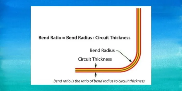
- Avoid Sharp Corners: Use 45-degree bends or curved traces to prevent signal reflection.
4. Ground Planes and Shielding
A solid ground plane is essential in RF PCB design to provide a low-impedance return path for signals and reduce EMI. Avoid splitting the ground plane under RF traces, as this can create loops that act like antennas, picking up noise.
Step-by-Step Guide to RF PCB Design for Beginners
This section offers a practical RF PCB design tutorial to help you create your first high-frequency board. Follow these steps to go from concept to a functional design.
Step 1: Define Your Specifications
Start by identifying the operating frequency, power levels, and application of your circuit. For example, a 2.4 GHz Wi-Fi module will have different requirements than a 900 MHz RFID system. Write down parameters like impedance (typically 50 ohms) and maximum signal loss (often less than 3 dB).
Step 2: Select Software Tools
Choose a PCB design software that supports RF simulations and impedance calculations. Many free or affordable tools are available online, offering features like schematic capture and layout design. Look for options with built-in calculators for trace width and spacing based on frequency.
Step 3: Create the Schematic
Design your circuit schematic, including RF components like amplifiers, filters, and antennas. Ensure you include decoupling capacitors near power pins to reduce noise—typically 0.1 μF for high-frequency applications.
Step 4: Design the Layout
Translate your schematic into a PCB layout, following the trace routing and ground plane guidelines mentioned earlier. Use vias to connect layers if needed, but minimize their use in RF paths to avoid inductance.
Step 5: Simulate and Test
Before manufacturing, simulate your design to check for signal integrity and impedance matching. Tools often provide S-parameter analysis to predict how your circuit will behave at the target frequency, such as 5 GHz for some wireless applications.
Step 6: Prototype and Iterate
Once your design is ready, produce a prototype and test it with equipment like a vector network analyzer (VNA) to measure parameters like return loss. If the results don’t meet your specs—say, a return loss worse than -10 dB—revise the layout and repeat the process.
Common Mistakes in RF PCB Design and How to Avoid Them
As a beginner, it’s easy to make errors in RF PCB design. Here are some pitfalls to watch out for, along with tips to avoid them.
1. Ignoring Impedance Control
Failing to calculate trace width for a 50-ohm impedance can lead to signal reflections. Use online calculators or software tools to determine the correct dimensions based on your board’s dielectric constant and thickness.
2. Poor Grounding Practices
Split ground planes or insufficient vias can introduce noise. Always use a continuous ground plane and place vias strategically to connect layers, ensuring a low-impedance path.
3. Overlooking Component Placement
Placing sensitive RF components near noisy digital circuits can cause interference. Group RF components together and isolate them from digital or power sections with shielding or distance.
Learning RF PCB Design Online: Resources for Beginners
If you’re looking for an RF PCB design course or ways to learn RF PCB design online, there are plenty of resources available to build your skills.
1. Free Tutorials and Guides
Many websites offer free RF PCB design tutorials that cover everything from theory to layout tips. Look for step-by-step guides with practical examples, like designing a simple RF amplifier.
2. Video Courses
Platforms like YouTube host detailed video series on RF PCB design for beginners. These often include visual demonstrations of software tools and real-world projects, making complex topics easier to grasp.
3. Community Forums
Join online communities where engineers share advice on RF PCB design challenges. These forums are great for troubleshooting specific issues, such as reducing EMI in a 433 MHz circuit.
Tips for Success in RF PCB Design
To wrap up this RF PCB design tutorial, here are some final tips to help you succeed as a beginner:
- Start with simple projects, like a low-power RF transmitter, before tackling complex designs.
- Invest time in learning software tools, as they can automate impedance calculations and simulations.
- Stay updated on industry standards for RF design, such as those for wireless protocols like Bluetooth or Zigbee.
- Collaborate with experienced designers through online platforms to gain insights and feedback.
Conclusion
RF PCB design may seem daunting for beginners, but with the right foundation, it becomes an achievable skill. This guide has covered the essentials of RF PCB design basics, from understanding high-frequency theory to applying practical layout techniques. Whether you’re following an RF PCB design course, exploring RF PCB design online, or using this RF PCB design tutorial as your starting point, remember that practice and patience are key.
By focusing on signal integrity, impedance matching, and proper grounding, you can create reliable RF circuits for a wide range of applications. Start small, test often, and keep learning to refine your skills in RF PCB design for beginners. With these tools and knowledge, you’re well on your way to mastering high-frequency electronics.