ALLPCB


Introduction
Designing and optimizing antennas is challenging. For industrial IoT antennas, a reference design can be a useful starting point. The question is which parameters can be adjusted to optimize a reference design for a final product.
Project Overview
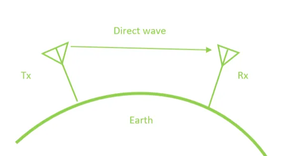
This article discusses a Bluetooth antenna design for an industrial IoT product. The design goal was to integrate a Bluetooth antenna into a product without a display and to use a smartphone app for configuration. The design approach is applicable to other product types as well.
Starting from a Reference Design
A Bluetooth antenna reference design from Cypress Semiconductor was identified online. Its documentation states it is for reference only and not intended as a finished product module. It was designed as a lab platform to enable software development in parallel with PCB design.
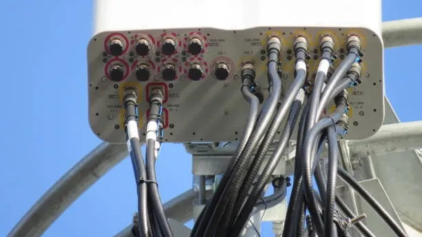
The schematic, BOM, and PCB layout were provided in Cadence Allegro format, making the design a suitable starting point for optimization. The reference used a large connector in the lab setup.
Design Objectives
The two main objectives were antenna miniaturization and performance optimization. Replacing the large connector with a rigid-flex PCB enables a smaller antenna structure, but the impact on antenna performance needed evaluation. A series of hypothesis-driven analyses were performed to understand these effects and to define a correct optimization strategy.
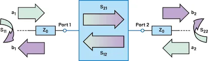
Simulation Results and Matching Network Optimization
Multiple analyses were run using discrete components available in the parts library and the selected PCB material parameters. Automated frequency sweeps showed improved impedance matching network performance. These simulation-driven improvements yielded about a 2 dB antenna performance increase prior to miniaturization.
Miniaturization Challenges: Grounding and Flex Regions
Adequate ground is critical in antenna design, so miniaturization presents challenges as the PCB ground plane area is reduced. In the reference design, the ground system consisted of two planes, several vias, and an external cable tied to ground.
Analysis of a small PCB section that houses the antenna and circuitry showed insufficient ground in the rigid area, causing the antenna to miss performance targets. Additional ground area was required in the flexible portion of the PCB. Modeling the flex part as a solid plane simplifies simulation and is quick to implement. Using a hatched pattern to allow bending without cutting copper greatly increases mesh size and simulation time.
Comparisons of different plane shapes and sizes showed that simplified geometries can be used for hypothesis analysis without significant error, although final simulations should be as accurate as possible.
Mechanical Clearance and Housing Effects
In a subsequent sweep, the minimum distance between the antenna and the plastic housing was evaluated. In this case, spacing greater than 10 mm had no further impact on antenna performance.
Flex Shape and Rigid PCB Mounting
Changing the flex part shape in 2D or by folding in 3D impacts performance. After fixing the mounting location and determining the flex length and shape, the next question was how to mount the rigid portion of the PCB.
A screw position sweep showed that mounting screw locations significantly affect antenna performance when placed at mechanically optimal positions. For alternative mounting methods, snap-fit options were considered, which required cutting the PCB.
Visualization of PCB current density indicated high currents at 90° corners or mounting holes, which can cause EMI issues. Additional optimization of corner geometry and mounting features was required to minimize EMI.
Final Outcome
The antenna was reduced to 53% of the original reference size while achieving a wider bandwidth and about a 6 dB improvement in PCB antenna performance.
The conclusion is that antenna miniaturization imposes stricter design constraints. Mechanical mounting details such as screw holes, clearances, housing materials, and EMI must be carefully considered. Optimizing these factors up front can reduce the need for additional prototype redesigns and shorten time to market.
Collaboration from Design to Measurement
Nor dc ad and FlowCAD collaborated on a state-of-the-art antenna amplifier and an inverted-F antenna module. Schematic capture and PCB layout were completed in Cadence Allegro PCB Designer.
After component optimization, impedance matching was achieved. Measurements of the physical design were performed with an R&S vector network analyzer and compared to simulation results.
This collaboration demonstrates effective coordination between theory, simulation, and measurement for predictable RF design.