 ALLPCB


When designing a printed circuit board (PCB), one of the key decisions is choosing the right copper foil thickness. This choice impacts performance, cost, and manufacturing ease. So, what are the copper foil pros and cons? Thicker copper offers benefits like higher current capacity and better heat dissipation but comes with higher costs and design challenges. On the other hand, thinner copper is cost-effective and easier to work with for fine traces, but it has drawbacks like limited current handling and potential reliability issues. Understanding copper thickness trade-offs is crucial for optimizing your PCB design.
In this comprehensive guide, we’ll dive deep into the benefits of thicker copper, the drawbacks of thinner copper, and the trade-offs you need to consider. Whether you’re an engineer or a hobbyist, this article will help you make informed decisions for your next project.
Why Copper Foil Thickness Matters in PCB Design
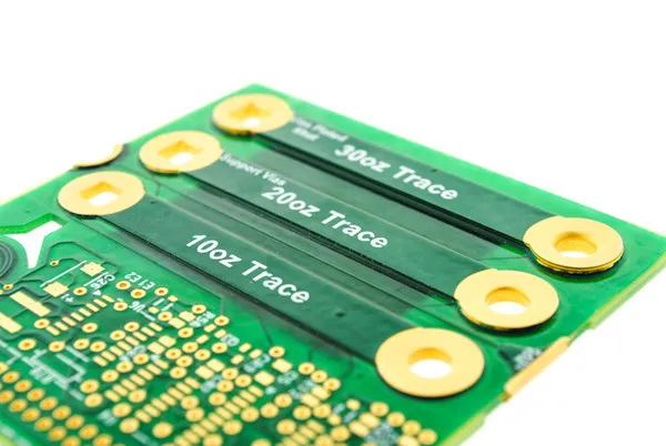
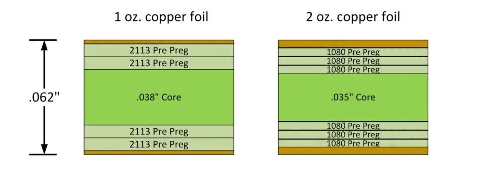
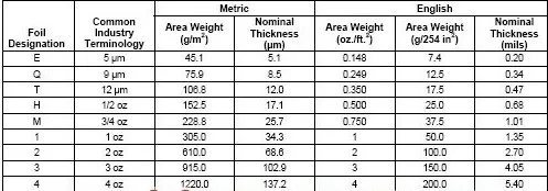
Copper foil thickness is a critical factor in PCB design because it directly affects how the board handles electrical current, heat, and signal integrity. Measured in ounces per square foot (oz/ft2), copper thickness typically ranges from 0.5 oz (about 17.5 micrometers) to 3 oz (about 105 micrometers) or more for specialized applications. A standard PCB often uses 1 oz copper, which strikes a balance between performance and cost.
The thickness you choose influences the board’s ability to carry current without overheating, maintain signal quality, and fit within physical design constraints. Let’s explore how different thicknesses impact your PCB and the trade-offs involved.
Benefits of Thicker Copper Foil in PCBs
Thicker copper foil, often 2 oz or more, is commonly used in high-power applications. Here are the key advantages of opting for thicker copper in your design.
1. Higher Current Carrying Capacity
One of the primary benefits of thicker copper is its ability to handle higher electrical currents without overheating. According to IPC standards, a 1 oz copper trace with a width of 10 mils can carry about 1.2 amps safely at a 10°C temperature rise. In contrast, a 2 oz copper trace of the same width can handle approximately 2.4 amps under similar conditions. This makes thicker copper ideal for power electronics, motor controllers, and automotive applications where high current is common.
2. Improved Thermal Management
Thicker copper dissipates heat more effectively due to its larger cross-sectional area. This is critical in designs where components generate significant heat, such as LED lighting systems or power supplies. By reducing thermal resistance, thicker copper helps prevent hotspots that could damage components or degrade performance over time.
3. Enhanced Mechanical Strength
In multi-layer PCBs or boards subjected to mechanical stress, thicker copper provides added durability. It can withstand vibrations and physical handling better than thinner copper, reducing the risk of trace cracking or delamination during assembly or use.
4. Better for High-Power Applications
For industries like renewable energy or industrial automation, thicker copper (often 3 oz or more) is essential. These applications demand robust current paths to support heavy loads, and thicker copper ensures reliability under demanding conditions.
Drawbacks of Thicker Copper Foil
While thicker copper offers significant advantages, it also comes with challenges that may not suit every project. Here are the main drawbacks to consider.
1. Higher Manufacturing Costs
Thicker copper requires more raw material, which increases the cost of production. Additionally, the etching process for thicker copper can be more complex and time-consuming, further driving up expenses. For budget-conscious projects or mass production, this can be a significant limitation.
2. Increased Board Weight and Thickness
Using thicker copper adds to the overall weight and thickness of the PCB. In applications like wearable electronics or aerospace, where size and weight are critical, this can be a major disadvantage. A board with 3 oz copper will be noticeably bulkier than one with 0.5 oz copper, potentially affecting the final product design.
3. Challenges with Fine Pitch Designs
Thicker copper is harder to etch precisely, making it less suitable for high-density interconnect (HDI) designs with fine traces and tight spacing. For modern electronics requiring compact layouts, such as smartphones or IoT devices, thinner copper is often a better choice.
Advantages of Thinner Copper Foil in PCBs
Thinner copper foil, typically 0.5 oz to 1 oz, is widely used in consumer electronics and low-power applications. Let’s look at its benefits.
1. Cost-Effective Solution
Thinner copper uses less material, making it a more affordable option for large-scale production. For projects where cost is a primary concern, such as simple gadgets or prototypes, thinner copper can save significant expenses without compromising basic functionality.
2. Easier to Etch for Fine Traces
Thinner copper allows for more precise etching, which is essential for creating narrow traces and small gaps in high-density designs. This is why 1 oz copper is the standard in many PCB designs—it offers a good balance of manufacturability and performance for intricate layouts.
3. Reduced Board Weight and Size
In applications where space and weight are limited, such as drones or portable devices, thinner copper helps keep the PCB lightweight and compact. This can be a critical factor in meeting design specifications for modern electronics.
4. Suitable for High-Frequency Signals
Thinner copper can be advantageous in high-frequency applications where signal integrity is a priority. It reduces parasitic capacitance and can help maintain consistent impedance, which is vital for RF circuits operating at frequencies above 1 GHz.
Drawbacks of Thinner Copper Foil
Despite its advantages, thinner copper has limitations that can impact performance and reliability. Here are the key drawbacks of thinner copper.
1. Limited Current Handling
Thinner copper cannot handle high currents as effectively as thicker copper. For instance, a 0.5 oz copper trace may only support around 0.6 amps for a 10 mil width at a 10°C temperature rise. This makes it unsuitable for power-intensive applications where overheating could lead to trace failure.
2. Poor Heat Dissipation
With less material to conduct heat away from components, thinner copper struggles to manage thermal loads. In designs with high-power components, this can result in overheating, reduced lifespan, or even catastrophic failure.
3. Increased Risk of Damage
Thinner copper is more prone to mechanical damage during manufacturing or use. It can crack or break under stress, especially in environments with vibration or frequent handling, leading to potential reliability issues.
4. Higher Susceptibility to Noise and Crosstalk
In high-density designs, thinner copper traces are more susceptible to electromagnetic interference (EMI) and crosstalk. This can degrade signal quality, particularly in sensitive analog or high-speed digital circuits.
Copper Thickness Trade-Offs: Finding the Right Balance
Choosing the right copper thickness for your PCB involves balancing performance, cost, and design requirements. Here are some key copper thickness trade-offs to keep in mind.
Performance vs. Cost
Thicker copper enhances current capacity and heat dissipation but increases production costs. If your application doesn’t require high power, opting for 1 oz copper can save money while still meeting performance needs. For high-power designs, the added cost of 2 oz or 3 oz copper may be justified by the improved reliability.
Design Complexity vs. Manufacturability
Thinner copper is ideal for complex, high-density designs with fine traces, but it may not support the current or thermal demands of your circuit. Thicker copper, while better for power handling, can limit how tightly you can pack components. Consider your layout constraints and manufacturing capabilities when deciding.
Application-Specific Needs
The intended use of your PCB plays a big role in copper thickness selection. For example, a PCB for a simple consumer gadget may work fine with 0.5 oz copper to keep costs low. However, a PCB for an industrial inverter may require 3 oz copper to handle heavy loads and ensure long-term durability.
How to Choose the Right Copper Thickness for Your PCB
Selecting the appropriate copper thickness depends on several factors specific to your project. Here are practical steps to guide your decision.
1. Assess Current Requirements
Calculate the maximum current your traces need to carry. Use tools like trace width calculators based on IPC-2221 standards to determine the minimum copper thickness and trace width needed to avoid overheating. For currents above 2 amps, consider at least 2 oz copper.
2. Evaluate Thermal Demands
Identify components that generate significant heat and ensure the copper thickness can dissipate it effectively. For high-power designs, thicker copper or additional thermal management solutions like vias and heat sinks may be necessary.
3. Consider Signal Integrity
For high-frequency or high-speed digital circuits, prioritize thinner copper to maintain consistent impedance (typically 50 ohms for RF designs) and reduce signal loss. However, ensure the thickness still supports the required current without risking damage.
4. Factor in Cost and Size Constraints
Balance performance with budget and physical design limits. If weight and space are critical, lean toward thinner copper. If cost isn’t a major concern and reliability is paramount, thicker copper may be worth the investment.
Common Copper Thickness Options and Their Applications
Here’s a quick overview of standard copper thicknesses and where they are typically used in PCB design.
- 0.5 oz (17.5 μm): Used in low-power, cost-sensitive applications like simple sensors or basic consumer electronics. Best for fine-pitch, high-density designs.
- 1 oz (35 μm): The industry standard for most PCBs, offering a balance of cost, performance, and ease of manufacturing. Suitable for general-purpose electronics.
- 2 oz (70 μm): Ideal for moderate power applications like LED drivers or small motor controllers, where higher current and heat dissipation are needed.
- 3 oz and above (105 μm+): Used in heavy-duty power electronics, automotive systems, and industrial equipment requiring robust current handling and thermal performance.
Conclusion: Making an Informed Choice on Copper Thickness
Understanding the advantages and disadvantages of different copper foil thicknesses is essential for creating a PCB that meets your performance, cost, and design goals. Thicker copper offers benefits like higher current capacity and better heat management but comes with increased costs and design limitations. Thinner copper is cost-effective and suitable for compact, high-frequency designs, yet it struggles with power handling and durability.
By carefully evaluating the copper thickness trade-offs and aligning your choice with the specific needs of your application, you can optimize your PCB for success. Whether you’re working on a low-cost prototype or a high-power industrial system, the right copper thickness will ensure reliability and efficiency in your design.
At ALLPCB, we’re committed to supporting your PCB projects with tailored solutions and expert guidance. Explore our resources and services to bring your designs to life with confidence.


