ALLPCB


In the fast-evolving world of electronics, designing high-density printed circuit boards (PCBs) with Ball Grid Array (BGA) components can be a complex task. One of the biggest challenges is ensuring BGA breakout signal integrity. Poor signal integrity can lead to data errors, system failures, or reduced performance in high-speed applications. So, how do you achieve optimal signal integrity in BGA breakouts? It comes down to careful planning, precise routing, and addressing key factors like impedance control and crosstalk.
In this comprehensive guide, we’ll dive deep into the techniques and considerations for maintaining signal integrity during BGA breakouts. From BGA breakout impedance control to minimizing BGA breakout crosstalk, we’ll explore practical strategies that engineers and PCB designers can apply to ensure reliable performance in high-density designs. Let’s get started with the essentials of BGA breakouts and why signal integrity matters.
Understanding BGA Breakouts and Signal Integrity
A BGA breakout refers to the process of routing signals from the densely packed pins (or balls) of a BGA component to other parts of the PCB. BGA packages are popular in modern electronics because they support high pin counts in a small footprint, making them ideal for compact, high-performance devices. However, the tight spacing and high pin density create significant challenges for maintaining signal integrity.
Signal integrity is the measure of how well a signal maintains its quality as it travels through a PCB. When signal integrity is compromised, issues like noise, distortion, or timing errors can occur, especially in high-speed designs where data rates often exceed 1 Gbps. For BGA breakouts, achieving signal integrity means ensuring that signals escape the dense grid of balls without interference or degradation.
In the following sections, we’ll break down the key techniques and considerations for optimizing BGA breakout signal integrity, focusing on impedance control, crosstalk reduction, and other critical design practices.
Key Challenges in BGA Breakout Design
Before diving into solutions, it’s important to understand the main challenges that impact BGA breakout signal integrity. These include:
- High Pin Density: BGA components often have hundreds or thousands of pins in a small area, leaving little room for routing traces without interference.
- Signal Crosstalk: Close proximity of traces can cause electromagnetic interference, leading to BGA breakout crosstalk and signal distortion.
- Impedance Mismatches: Variations in trace width, layer transitions, or vias can disrupt impedance, causing reflections and signal loss.
- High-Speed Requirements: Modern applications often operate at frequencies above 500 MHz, where even small design flaws can lead to significant signal degradation.
Addressing these challenges requires a combination of strategic design practices and advanced tools. Let’s explore the most effective techniques for ensuring signal integrity in BGA breakouts.
Techniques for Achieving BGA Breakout Signal Integrity
1. Strategic Fanout and Routing Planning
The first step in a successful BGA breakout is planning the fanout, which is the pattern used to route signals away from the BGA balls. A well-designed fanout minimizes congestion and reduces the risk of signal interference. There are two common fanout strategies:
- Dog-Bone Fanout: This involves routing signals from the outer rows of BGA balls directly outward, while inner balls are connected to vias that route to other layers. This method works well for BGAs with a pitch of 1.0 mm or larger.
- Via-in-Pad Fanout: For finer pitch BGAs (below 0.8 mm), vias are placed directly under the BGA pads to route signals to inner layers. This reduces trace length and helps maintain signal integrity.
When planning fanout, prioritize high-speed signals by routing them on the shortest paths and avoiding unnecessary vias, which can introduce inductance and affect signal quality.
2. BGA Breakout Impedance Control
Impedance control is critical for maintaining BGA breakout signal integrity, especially in high-speed designs. Impedance mismatches can cause signal reflections, leading to data errors or loss. To achieve proper BGA breakout impedance control, consider the following:
- Trace Width and Spacing: Design traces to match the target impedance, typically 50 ohms for single-ended signals or 100 ohms for differential pairs. Use impedance calculators or simulation tools to determine the correct trace width based on your PCB stack-up and dielectric material.
- Layer Stack-Up Design: Place high-speed signal layers adjacent to ground planes to create a controlled impedance environment. For example, a 6-layer PCB might have signal layers sandwiched between ground planes to minimize noise.
- Via Transitions: Minimize the number of vias in high-speed signal paths, as each via can introduce a small impedance discontinuity. When vias are necessary, use back-drilling to remove unused via stubs, which can cause reflections.
By maintaining consistent impedance across the signal path, you can significantly reduce reflections and ensure reliable data transmission at speeds exceeding 2.5 Gbps.
3. Minimizing BGA Breakout Crosstalk
Crosstalk occurs when signals on adjacent traces interfere with each other, a common issue in dense BGA breakouts. Reducing BGA breakout crosstalk involves careful layout and routing practices, such as:
- Trace Spacing: Increase the spacing between adjacent traces to at least three times the trace width (3W rule) to minimize electromagnetic coupling. For example, if your trace width is 5 mils, maintain a spacing of 15 mils or more.
- Ground Planes and Guard Traces: Use continuous ground planes under signal layers to provide a return path and reduce crosstalk. Adding guard traces (grounded traces between signal lines) can further isolate high-speed signals.
- Differential Pair Routing: For differential signals, route pairs closely together with consistent spacing to maintain common-mode noise rejection, while keeping them away from other signal traces.
Simulation tools can help identify potential crosstalk issues before manufacturing. By addressing BGA breakout crosstalk early in the design phase, you can avoid costly redesigns and ensure signal quality.
4. Power and Ground Plane Design
A robust power distribution network (PDN) is essential for signal integrity in BGA breakouts. Poor power and ground design can introduce noise and affect signal quality. Follow these best practices:
- Decoupling Capacitors: Place decoupling capacitors close to BGA power pins to filter high-frequency noise. For a BGA with 100 power pins, you might need multiple capacitors with values ranging from 0.1 μF to 10 μF to cover different frequency ranges.
- Ground Plane Integrity: Avoid splitting ground planes under BGA components, as this can disrupt return paths and increase noise. Use a solid ground plane for reference.
- Power Plane Vias: Ensure sufficient vias connect power pins to power planes to minimize voltage drops, especially for high-current applications drawing over 5 Amps.
A well-designed PDN reduces noise and supports stable signal transmission, particularly for high-speed BGA breakouts.
5. High-Density Interconnect (HDI) Design
For extremely dense BGA packages with pitches below 0.5 mm, traditional routing may not be feasible. High-Density Interconnect (HDI) technology offers a solution by using microvias and finer traces to route signals in tight spaces. HDI design benefits include:
- Reduced trace lengths for better signal integrity.
- More layers for routing complex BGA breakouts.
- Smaller via sizes (e.g., 0.1 mm diameter) to fit within fine-pitch BGA pads.
While HDI increases manufacturing costs, it’s often necessary for cutting-edge designs requiring optimal BGA breakout signal integrity.
Additional Considerations for BGA Breakout Signal Integrity
Beyond the core techniques, several other factors play a role in maintaining signal integrity during BGA breakouts. These include:
- Material Selection: Choose PCB materials with low dielectric loss (e.g., FR-4 with a loss tangent of 0.02 or lower) for high-frequency applications to minimize signal attenuation.
- Simulation and Testing: Use signal integrity simulation tools to model BGA breakout performance before fabrication. Post-manufacturing testing with oscilloscopes can verify signal quality at speeds up to 10 Gbps.
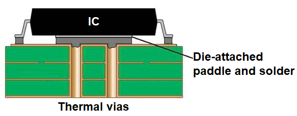
- Thermal Management: Ensure proper heat dissipation for BGA components, as excessive heat can affect signal performance. Use thermal vias or heat sinks if the BGA dissipates more than 2 Watts.
By considering these factors alongside core design techniques, you can create robust BGA breakouts that perform reliably under demanding conditions.
Tools for Optimizing BGA Breakout Designs
Modern PCB design software offers powerful features to simplify BGA breakout design and ensure signal integrity. Look for tools with:
- Automated fanout and routing wizards to streamline BGA breakout planning.
- Impedance calculators for precise BGA breakout impedance control.
- Signal integrity analysis to predict and mitigate issues like crosstalk and reflections.
Using these tools can save time and reduce errors, especially for complex designs with hundreds of BGA pins.
Conclusion: Mastering BGA Breakout Signal Integrity
Achieving optimal BGA breakout signal integrity is a critical aspect of designing high-density, high-speed PCBs. By focusing on strategic fanout, BGA breakout impedance control, and minimizing BGA breakout crosstalk, you can ensure that signals remain clear and reliable even in the most challenging layouts. Additional considerations like power plane design, HDI technology, and material selection further enhance performance.
Whether you’re working on consumer electronics, telecommunications, or industrial systems, the techniques and considerations outlined in this guide provide a roadmap for success. With careful planning, the right tools, and attention to detail, you can tackle the complexities of BGA breakouts and deliver designs that meet the demands of modern technology.
Start applying these strategies in your next project to see the difference in signal quality and overall system reliability. With the right approach, even the most intricate BGA designs can achieve outstanding performance.