ALLPCB


Overview
Chips are the core components of modern electronic products, acting as the "brain" of a system. Their development is technology- and capital-intensive, and manufacturing lines often require investments in the hundreds of millions to billions of US dollars. The complete chip manufacturing process includes chip design, wafer fabrication, packaging, and testing, and each stage represents significant technical complexity. Since the advent of EDA tools in the 1980s, automated chip design has reduced the manual difficulty of very-large-scale integration: designers describe functionality in hardware description languages, EDA tools compile that into logic, and the result is iteratively debugged and refined. Modern chips contain tens of billions of transistors; without EDA tools, high-end chip design would be impractical. Nevertheless, the availability of EDA does not make chip design easy: it remains a complex systems engineering task that integrates advanced techniques across multiple domains.
1. Architecture design
Architecture design is a major challenge. Even for relatively simple digital integrated circuits, design typically follows a top-down methodology and involves multiple stages:
- Requirements definition: combine analysis of external environment, supply chain resources, and company positioning to define product requirements, functions, expected board count, and integrated circuit types. The difficulty lies in accurately forecasting market and technology trends and understanding the capabilities of the design team and manufacturing partners.
- Function implementation: describe the functions the chip must realize, usually in a hardware description language. The difficulty is balancing achievable performance and functionality: meeting targets without exceeding the team or process limits.
- Structural design: partition the chip into submodules with clear interfaces and independent functions. The difficulty is achieving requirements with as few modules and as low complexity as possible.
- Logic synthesis: translate HDL into logic netlists. This stage demands synthesizable, clear, and maintainable code while considering module reuse.
- Physical implementation: map the logical netlist to physical connections according to the chosen process, minimizing components and interconnects to meet area and timing constraints while preventing internal interference.
- Physical layout: generate GDSII files for the foundry to implement the circuits on silicon, followed by packaging and testing to produce physical chips.
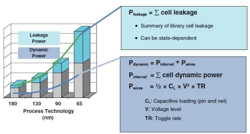
Design must account for many variables such as signal interference and thermal distribution. Physical effects like electromagnetic interactions vary significantly across processes and cannot always be derived from closed-form formulas or copied from existing data. Design teams rely on EDA tools for iterative simulation and tradeoffs; when simulation results are unsatisfactory, designs must be revised and retested, imposing heavy demands on engineering time and expertise.
2. Verification
Verification aims to discover hardware and software functional errors, optimize performance and power, and ensure the design meets its specifications before fabrication. Verification is not a single step after design but an ongoing, repetitive activity across all stages. It includes system-level verification, digital logic functional verification, mixed-signal verification, software verification, physical verification, and timing verification.
Verification is difficult for several reasons. First, verification can only falsify hypotheses; designers must anticipate likely failure modes and sometimes apply formal verification to increase confidence, which requires extensive experience. Second, verification methods must be efficient: chips now integrate processors, analog and digital IP, and memory interfaces, causing verification complexity to grow exponentially. Delivering comprehensive, debuggable verification prior to tape-out is a major engineering challenge. Third, verification itself can be costly. For example, in the 1990s FPGA-based verification supported up to about 2 million gates at roughly $1 per gate. Although unit prices have fallen, the gate counts for modern chips have risen to tens of millions or hundreds of millions, driving up total verification costs substantially.
3. Tape-out and prototype production costs
Tape-out (small-batch fabrication for testing) is technically part of manufacturing but is also a critical phase for design organizations. While tape-out uses existing process technologies and does not always require extensive foundry guidance, its primary constraint is cost. For example, using public pricing from CMP (Circuits Multi-Projects), and taking a die size comparable to a widely known processor (Qualcomm Snapdragon 855, die area 73.27 mm2), a 28 nm tape-out is quoted at 499,072.5 euros. That converts to a substantial local-currency amount. The result for a design organization can be a limited number of dies per run, and the per-die cost remains high. Moreover, tape-out is rarely a one-time event: failures require redesign and re-tape-out, and even successful runs often lead to further optimizations and additional tape-outs. Each cycle can cost on the order of millions in local currency, making funding a significant barrier to progress.
4. Increasing design demands
Design challenges are intensifying as chips are applied to AI, cloud computing, autonomous vehicles, 5G, and other domains. Security and reliability have become more critical, imposing stricter design constraints. Rapid development in AI and automotive electronics drives demand for domain-specific architectures and specialized accelerators, introducing new architectural challenges. At the same time, as silicon scaling approaches physical limits (the article notes projections toward subnanometer-level processes in the coming years), further performance gains and power reductions increasingly depend on innovative design techniques rather than process improvements. Process advances also require increased design guidance, adding further pressure on designers.