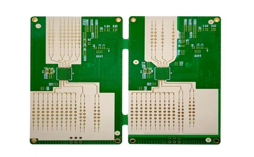
There! If you're looking to unlock high-power density in your designs with Direct Bonded Copper (DBC) PCBs, you've come to the right place. DBC PCBs are a game-changer for high power PCB design, offering exceptional thermal performance and the ability to handle high currents in power module applications. In this guide, we'll dive deep into the advantages of direct bonded copper, explore its thermal benefits, and provide practical insights for engineers working on high current PCB projects. Let's get started with everything you need to know about DBC technology!
In the fast-evolving world of power electronics, achieving high-power density while maintaining reliability is a constant challenge for engineers. As devices become smaller and more powerful, managing heat and ensuring efficient current flow are critical. This is where Direct Bonded Copper (DBC) PCBs shine. Renowned for their superior thermal performance and ability to handle high currents, DBC PCBs are a top choice for high power PCB design in applications like power modules, electric vehicles, and renewable energy systems.
In this comprehensive guide, we'll explore the ins and outs of DBC technology, focusing on its advantages, thermal management capabilities, and practical applications in high current PCB designs. Whether you're designing a compact power module PCB or tackling complex power electronics, this blog will equip you with the knowledge to leverage DBC for optimal performance.
What Are Direct Bonded Copper (DBC) PCBs?
Direct Bonded Copper (DBC) PCBs are specialized substrates designed for high-power applications. Unlike traditional PCBs that use adhesive layers to bond copper to the substrate, DBC technology bonds copper directly to a ceramic material, such as alumina (Al?O?) or aluminum nitride (AlN), through a high-temperature process. This creates a strong, reliable connection without intermediary layers, resulting in exceptional thermal conductivity and electrical insulation.
The process involves heating copper and the ceramic substrate in a controlled environment, forming a copper-oxygen eutectic layer that bonds the two materials. This direct bonding eliminates thermal resistance caused by adhesives, making DBC an ideal choice for high power PCB design where heat dissipation is a priority.
Why Choose DBC for High Power PCB Design?
When it comes to high-power electronics, the choice of substrate can make or break your design. DBC PCBs stand out for several reasons, offering unique benefits that cater to the demands of power module PCB applications and high current PCB projects. Let's break down the key advantages of direct bonded copper technology.
1. Superior Thermal Performance
One of the standout features of DBC PCBs is their exceptional thermal conductivity, often referred to as DBC thermal performance. The ceramic substrates used in DBC, such as aluminum nitride, can achieve thermal conductivity values ranging from 170 to 200 W/m·K, far surpassing traditional FR4 materials (around 0.3 W/m·K). This means heat generated by high-power components is quickly transferred away, reducing the risk of overheating and improving device reliability.
For instance, in a power module PCB for an electric vehicle inverter, efficient heat dissipation is crucial to prevent thermal runaway. DBC substrates ensure that heat from power semiconductors like IGBTs or MOSFETs is effectively managed, maintaining optimal operating temperatures even under heavy loads.
2. High Current Carrying Capacity
DBC PCBs are built to handle high currents, making them a go-to solution for high current PCB designs. The thick copper layers, often ranging from 0.1 mm to 0.3 mm, provide low electrical resistance and can support current densities exceeding 100 A/cm2 in some configurations. This capability is essential for applications like industrial motor drives or renewable energy converters, where high current flow is a constant demand.
Unlike standard PCBs where trace width limitations can bottleneck current capacity, DBC allows for robust copper patterns that minimize voltage drops and power losses, ensuring efficient energy transfer.
3. Excellent Electrical Insulation
The ceramic layer in DBC PCBs provides outstanding electrical insulation, with dielectric breakdown voltages often exceeding 10 kV/mm. This property is critical in high-power applications where components operate at high voltages. The insulation prevents short circuits and ensures safe operation, even in compact designs with tight spacing.
4. Mechanical Stability and Durability
DBC substrates are known for their mechanical strength and resistance to thermal cycling. The direct bonding process creates a robust structure that can withstand temperature fluctuations without delamination or cracking. This durability is vital for power electronics in harsh environments, such as automotive or aerospace systems, where components face extreme conditions.
Applications of DBC PCBs in Power Electronics
The unique properties of DBC PCBs make them indispensable in various high-power applications. Here are some key areas where DBC technology excels, particularly in high power PCB design and power module PCB development.
1. Electric Vehicle (EV) Power Systems
In electric vehicles, power inverters and converters manage high currents and voltages to drive motors efficiently. DBC PCBs are widely used in these systems due to their ability to handle power levels exceeding 100 kW while dissipating heat effectively. Their compact design also helps reduce the size and weight of EV powertrains, contributing to better vehicle efficiency.
2. Renewable Energy Systems
Solar inverters and wind turbine controllers rely on power module PCBs to convert and manage energy. DBC substrates ensure reliable operation under high-power conditions, with thermal performance that prevents overheating during peak loads. For example, a solar inverter using DBC can maintain efficiency even when processing currents of 50 A or more.
3. Industrial Power Electronics
From motor drives to welding equipment, industrial applications demand robust high current PCB solutions. DBC PCBs support the high-power density required for these systems, ensuring consistent performance and longevity despite continuous operation at elevated temperatures.
4. Aerospace and Defense
In aerospace and defense, reliability under extreme conditions is non-negotiable. DBC PCBs are used in radar systems, power supplies, and communication equipment, where their thermal and mechanical stability ensures uninterrupted operation in challenging environments.
Design Considerations for DBC PCBs in High Power Applications
While DBC PCBs offer numerous advantages, designing with this technology requires careful planning to maximize performance. Below are key considerations for engineers working on high power PCB design and high current PCB projects using DBC substrates.
1. Material Selection
Choosing the right ceramic material is critical for DBC thermal performance. Alumina (Al?O?) is cost-effective and offers good thermal conductivity (around 24-30 W/m·K), suitable for many applications. However, for designs requiring higher heat dissipation, aluminum nitride (AlN) with conductivity up to 200 W/m·K is a better choice, despite its higher cost.
2. Copper Thickness and Patterning
The thickness of the copper layer directly impacts current-carrying capacity and thermal spreading. Thicker copper (e.g., 0.3 mm) is ideal for high current PCB designs but may increase manufacturing complexity. Additionally, copper patterns should be optimized to minimize resistance and ensure even heat distribution across the board.
3. Thermal Interface with Heat Sinks
To fully leverage DBC thermal performance, proper integration with heat sinks or cooling systems is essential. The bottom copper layer of a DBC PCB is often soldered to a heat spreader or baseplate, ensuring efficient heat transfer. Thermal interface materials (TIMs) with low thermal resistance (e.g., below 0.5 K/W) should be used to enhance this connection.
4. Managing Thermal Expansion
Ceramic and copper have different coefficients of thermal expansion (CTE), which can cause stress during temperature changes. To mitigate this, designers should consider symmetrical copper layering (copper on both sides of the ceramic) to balance stress and prevent warping. For instance, a CTE mismatch between copper (17 ppm/K) and alumina (7 ppm/K) can be managed with careful design to avoid cracking over time.
Challenges and Limitations of DBC PCBs
While DBC PCBs are a powerful solution for high power PCB design, they are not without challenges. Understanding these limitations helps engineers make informed decisions when selecting substrates for power module PCB projects.
1. Higher Manufacturing Costs
The specialized bonding process and materials used in DBC PCBs result in higher costs compared to standard FR4 boards. For small-scale or cost-sensitive projects, this can be a barrier, though the performance benefits often justify the investment in high-power applications.
2. Limited Design Flexibility
DBC substrates are rigid and primarily suited for planar designs, limiting their use in flexible or multi-layer PCB configurations. Engineers may need to combine DBC with other technologies for complex systems requiring intricate routing.
3. Size Constraints
DBC PCBs are typically used in smaller, high-power sections of a design rather than large, multi-functional boards. Their manufacturing process also limits the maximum size of the substrate, which may require tiling multiple DBC sections for larger applications.
How DBC PCBs Compare to Other High-Power Substrates
To fully appreciate the direct bonded copper advantages, it's helpful to compare DBC with other substrates used in high power PCB design, such as Metal Core PCBs (MCPCBs) and Insulated Metal Substrates (IMS).
- DBC vs. MCPCBs: While MCPCBs use a metal base (often aluminum) for heat dissipation, they rely on a dielectric layer that introduces thermal resistance. DBC's direct bonding offers better thermal conductivity (up to 200 W/m·K vs. 1-5 W/m·K for MCPCBs), making it superior for extreme high-power applications.
- DBC vs. IMS: IMS substrates also use a metal base with a thin dielectric layer, but their thermal performance lags behind DBC due to the insulating layer's limitations. DBC is preferred for applications requiring both high thermal performance and electrical insulation.
In short, DBC stands out for its unmatched combination of thermal management and high current capacity, though cost and design constraints may lead engineers to consider alternatives for less demanding projects.
Tips for Optimizing DBC PCB Performance
To get the most out of DBC technology in your high current PCB or power module PCB designs, consider these practical tips:
- Simulate Thermal Behavior: Use thermal simulation tools to predict heat distribution and identify potential hotspots before manufacturing. This can save time and costs by optimizing the design early.
- Partner with Experienced Manufacturers: The precision required for DBC bonding demands expertise. Collaborate with a trusted PCB provider to ensure high-quality substrates tailored to your specifications.
- Balance Cost and Performance: For applications with moderate power needs, consider hybrid designs that combine DBC for critical high-power sections with standard materials for less demanding areas.
- Test Under Real Conditions: Validate your DBC PCB design with real-world testing to confirm thermal and electrical performance, especially for mission-critical applications like automotive or aerospace systems.
Future Trends in DBC Technology for High Power PCB Design
As power electronics continue to advance, DBC technology is evolving to meet new demands. Innovations in ceramic materials, such as silicon nitride (Si?N?), promise even higher thermal conductivity and mechanical strength, potentially exceeding 100 W/m·K while maintaining cost efficiency. Additionally, advancements in manufacturing techniques are reducing production costs, making DBC more accessible for a wider range of applications.
The rise of wide-bandgap semiconductors like SiC and GaN, which operate at higher temperatures and voltages, is also driving demand for DBC substrates. These materials require exceptional thermal management, and DBC's ability to handle extreme conditions positions it as a key enabler for next-generation power systems.
Conclusion: Harnessing DBC for High-Power Density
Direct Bonded Copper (DBC) PCBs are a cornerstone of modern high power PCB design, offering unmatched thermal performance, high current capacity, and reliability for power module PCB applications. From electric vehicles to renewable energy systems, DBC substrates empower engineers to push the boundaries of power density while keeping heat and electrical challenges in check.
By understanding the direct bonded copper advantages and incorporating best practices into your designs, you can unlock the full potential of DBC technology. Whether you're tackling a high current PCB project or optimizing a compact power module, DBC provides the foundation for efficient, durable, and high-performing electronics.
Ready to elevate your power electronics with DBC PCBs? Dive into this technology and see how it transforms your designs into cutting-edge solutions for today's high-power demands.
 ALLPCB


