ALLPCB


Overview
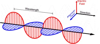
Because of transformer construction, there is a distributed capacitance between the primary and secondary windings. This distributed capacitance is one of the reasons for leakage flux.
This article briefly analyzes how an inter-winding shield layer between the primary and secondary windings in a switching power supply affects product EMI.
Part 1: Observed Phenomenon
The typical internal structure of a switching power supply is shown below. In some designs the primary and secondary windings are separated by a shielding material, commonly copper foil, and the shield is connected by a conductor to the primary-side reference ground plane.
With a shielded isolation transformer installed, radiation emission and conducted disturbance tests passed the CLASS B limits specified in EN55022. The measured spectra showed compliance for both radiation and conducted emissions when the shielded transformer was used.
When the isolation transformer was replaced with a non-shielded transformer, both radiation emission and conducted disturbance tests exceeded the limits.
Part 2: Root Cause Analysis
As the name implies, a switching power supply performs voltage conversion by switching power transistors. One of the main EMI sources is the switching circuit itself.
The switching circuit consists of the power switch and the high-frequency transformer. When the power switch turns on and off it generates high-amplitude pulses similar to PWM. Those pulses have a wide spectral band and rich harmonics. The disturbance propagation can be summarized as follows.
The switch drives the transformer primary, which is an inductive load. At the instant the switch turns on, the di/dt in the primary winding is largest and a surge spike appears across the primary winding.
When the switch turns off, leakage flux in the primary prevents some energy from transferring to the secondary. The energy stored in the inductance combines with capacitances and resistances in the collector circuit to produce a damped oscillation with spikes superimposed on the turn-off voltage, resulting in turn-off voltage spikes.
Turn-off of the power switch produces a large di/dt similar to the turn-on event, which generates significant noise (U = L * di/dt). This noise couples via distributed capacitance to input and output terminals and forms conducted disturbances.
The high-frequency switching current loop formed by the transformer primary, the power switch, and filter capacitors can generate significant spatial radiation and produce radiated disturbance. Therefore, layout in this area must minimize loop area.
If the filter capacitor value is insufficient or its high-frequency characteristics are poor, the capacitor impedance at high frequency can cause high-frequency current to flow into the AC supply as differential-mode current and produce conducted disturbance.
Distributed capacitance between the transformer primary and secondary allows noise from the primary loop to be transferred to the secondary loop. This increases the disturbance coupling path and can cause the LISN to receive more current, making conducted disturbance measurements exceed limits. The distributed-capacitance equivalent circuit shows how the coupling increases disturbance transfer.
If a shield layer is added inside the transformer and connected to the primary reference ground, the shield effectively interrupts the noise transfer path and reduces the disturbance loop area. That suppresses both conducted and radiated emissions. The shield location corresponds to point A in the equivalent circuit diagrams.
Part 3: Mitigation Measures
From the analysis above, when a switching power supply exhibits radiated or conducted disturbance issues, take the following steps:
- Check whether the transformer is unshielded. If so, replace it with a shielded transformer and ensure the shield is connected to the primary reference ground.
- To ensure the shield provides effective isolation, the connection between the shield and reference ground should present near-zero impedance. This is key to judging shield effectiveness.
- In practice, a single metal conductor without gaps or vias, with an aspect ratio less than 5, exhibits very low impedance.
Part 4: Considerations and Takeaways
A shielded transformer can effectively suppress common-mode noise from propagating from the switching stage to downstream circuitry.
This shield functions primarily as an electrostatic shield rather than a general magnetic shield, so the shield should be grounded or connected to the reference node.
A conductor used for electromagnetic shielding can in principle be left floating, but a floating electrostatic shield can accumulate charge and produce a "negative electrostatic shielding" effect, which is undesirable.
Power switches and output diodes often dissipate significant power and are mounted on heatsinks. Thermal interface materials such as thermal grease create distributed capacitance between the heatsink and the device, and between the heatsink and the chassis. That distributed capacitance can couple EMI to the AC input as common-mode disturbance, so heatsinks are commonly tied to reference ground.
Grounding heatsinks also prevents floating metal from acting as an unintended radiator and causing radiated emission failures. For more on floating metal effects on radiated emissions, see the previous EMC test case analysis article "EMC Test Case Analysis - Effect of Floating Metal on Radiated Emission".