ALLPCB


In the world of printed circuit board (PCB) design, achieving optimal performance and reliability is a constant challenge. One key factor that significantly influences both signal integrity and physical stability is stackup symmetry. A symmetrical PCB stackup refers to a balanced arrangement of layers in a PCB, ensuring uniformity in material distribution and thickness. But how does this impact signal integrity and prevent issues like warpage? Simply put, a balanced stackup design minimizes electrical interference and mechanical stress, leading to better signal quality and reduced risk of deformation during manufacturing and operation. In this blog, we’ll dive deep into the importance of balanced stackup design, explore its effects on signal integrity and stackup symmetry, and discuss techniques for PCB warpage prevention, including addressing CTE mismatch in stackup.
What Is Stackup Symmetry and Why Does It Matter?
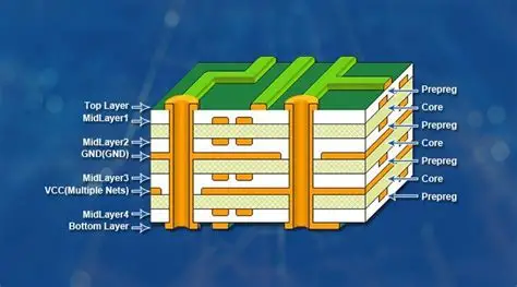
Stackup symmetry in PCB design refers to the even distribution of copper layers, dielectric materials, and thicknesses across the board’s cross-section. Imagine a sandwich where each slice of bread and filling is perfectly aligned and balanced. In a PCB, this balance ensures that the board behaves predictably under electrical and thermal conditions. A symmetrical PCB stackup typically mirrors layers around the center of the board, with equal numbers of signal, ground, and power planes on either side.
Why is this important? Without symmetry, a PCB can face two major issues: degraded signal integrity and physical warpage. Signal integrity refers to the quality of electrical signals as they travel through the board, while warpage is the bending or twisting of the board due to uneven stress. A balanced design tackles both by reducing electromagnetic interference (EMI) and minimizing mechanical strain caused by temperature changes. Let’s break down these impacts in detail.
How Stackup Symmetry Enhances Signal Integrity
Signal integrity and stackup symmetry are closely linked because the arrangement of layers directly affects how signals propagate through a PCB. Signal integrity issues, such as crosstalk, noise, and impedance mismatches, can lead to data errors or system failures, especially in high-speed designs. Here’s how symmetry helps:
- Consistent Impedance Control: In a symmetrical stackup, the dielectric thickness and copper distribution are uniform, ensuring consistent characteristic impedance for signal traces. For instance, a high-speed signal operating at 5 GHz requires a controlled impedance of typically 50 ohms. Symmetry helps maintain this value across the board, reducing signal reflections.
- Reduced Crosstalk: By placing ground planes symmetrically adjacent to signal layers, a balanced stackup minimizes crosstalk—the unwanted coupling of signals between traces. A typical 6-layer PCB might have a stackup like Signal-Ground-Power-Power-Ground-Signal, ensuring each signal layer is shielded.
- Lower EMI: Symmetry in layer arrangement helps create a uniform return path for signals, reducing electromagnetic interference. This is critical for designs operating in noisy environments or at high frequencies above 1 GHz.
In practice, achieving perfect symmetry can be challenging, especially in complex multilayer boards. However, even partial symmetry, where key layers like ground and power are balanced, can significantly improve signal quality. For high-speed designs, simulation tools can predict impedance values and signal behavior, allowing designers to fine-tune the stackup before fabrication.
The Role of Stackup Symmetry in PCB Warpage Prevention
Warpage is a physical deformation of the PCB that occurs due to uneven stress during manufacturing or operation. This can lead to assembly issues, such as poor soldering, or even complete board failure. PCB warpage prevention is a critical consideration, and stackup symmetry plays a vital role in minimizing this risk. Here’s how:
- Balanced Thermal Expansion: Different materials in a PCB expand and contract at different rates when exposed to heat. This is known as the Coefficient of Thermal Expansion (CTE). A CTE mismatch in stackup—where materials on one side of the board expand more than the other—can cause warpage. A symmetrical design ensures that materials with similar CTE values are distributed evenly, reducing stress. For example, FR-4, a common PCB material, has a CTE of about 14-17 ppm/°C in the X-Y direction, while copper has a CTE of 17 ppm/°C. Balancing these materials across layers prevents uneven expansion.
- Uniform Copper Distribution: Copper density variations between layers can lead to uneven heating and cooling during soldering or operation. A balanced stackup design ensures that copper coverage is mirrored across the board’s thickness, minimizing thermal gradients that cause bending.
- Even Layer Thickness: Symmetrical stackups maintain consistent dielectric and copper thicknesses on both sides of the center plane. For instance, in an 8-layer PCB, if the top four layers mirror the bottom four in terms of material and thickness, the board is less likely to warp under thermal stress.
Warpage isn’t just a manufacturing issue; it can also occur during the board’s lifecycle due to repeated thermal cycling. By prioritizing symmetry early in the design phase, engineers can avoid costly redesigns and ensure long-term reliability.
Addressing CTE Mismatch in Stackup for Warpage Control
One of the most common causes of warpage is a CTE mismatch in stackup. CTE, or Coefficient of Thermal Expansion, measures how much a material expands or contracts with temperature changes. When materials with significantly different CTE values are unevenly distributed in a PCB, the board can bend or twist as it heats up or cools down. Let’s explore how to address this in a symmetrical design:
- Material Selection: Choose materials with similar CTE values for adjacent layers. For example, pairing FR-4 with copper is generally safe due to their close CTE values. However, if a high-frequency material like Rogers 4350B (CTE of 10-12 ppm/°C) is used on one side and FR-4 on the other, asymmetry in expansion can occur. A symmetrical stackup balances these materials across the board.
- Layer Pairing: Mirror layers with high CTE mismatch on opposite sides of the board’s center. This ensures that any expansion or contraction is counteracted by an equal force on the other side, maintaining flatness.
- Thermal Simulation: Use design software to simulate thermal behavior before fabrication. These tools can predict warpage risks by analyzing CTE values and layer arrangements, allowing adjustments to achieve symmetry.
By carefully managing CTE differences through a balanced stackup design, manufacturers can significantly reduce warpage, ensuring the board remains flat and functional even under harsh conditions.
Practical Tips for Designing a Symmetrical PCB Stackup
Creating a symmetrical PCB stackup requires careful planning and attention to detail. Here are some actionable tips to guide engineers in achieving balance for both signal integrity and warpage prevention:
- Start with an Even Number of Layers: Whenever possible, design with an even number of layers (e.g., 4, 6, 8) to make symmetry easier. For example, a 6-layer board can be arranged as Signal-Ground-Power-Power-Ground-Signal, ensuring balance.
- Mirror Copper and Dielectric Layers: Ensure that copper density and dielectric thickness are mirrored around the board’s center. If the top layer has 1 oz copper, the bottom layer should match it.
- Place Ground Planes Strategically: Position ground planes next to signal layers to provide shielding and maintain impedance control. This also helps with symmetry if mirrored correctly.
- Consider Manufacturing Constraints: Work closely with your fabrication partner to understand material availability and layer thickness options. Some materials or thicknesses may not support perfect symmetry, so adjustments may be needed.
- Test and Validate: Use simulation tools to analyze signal integrity and thermal behavior. For high-speed designs, aim for impedance values within ±10% of the target (e.g., 50 ohms ±5 ohms), and check for warpage risks under temperature ranges like 25°C to 125°C.
These steps can help create a robust design that balances electrical performance with physical stability, addressing both signal integrity and stackup symmetry as well as PCB warpage prevention.
Challenges in Achieving Stackup Symmetry
While the benefits of a symmetrical PCB stackup are clear, achieving perfect balance isn’t always straightforward. Here are some common challenges and how to address them:
- Complex Designs: High-layer-count PCBs (e.g., 16 or more layers) often require specific layer arrangements for routing or power distribution, making symmetry difficult. In such cases, focus on partial symmetry by balancing critical layers like ground and power planes.
- Material Limitations: Not all materials have matching CTE values or thicknesses, leading to potential CTE mismatch in stackup. Collaborate with material suppliers to find compatible options or use thermal simulations to predict and mitigate issues.
- Cost Constraints: Symmetrical designs may require additional layers or specific materials, increasing costs. Balance performance needs with budget by prioritizing symmetry in critical areas of the board.
Despite these challenges, the long-term benefits of a balanced design—such as improved reliability and reduced rework—often outweigh the initial hurdles.
Conclusion: Prioritizing Symmetry for PCB Success
In summary, stackup symmetry is a cornerstone of high-quality PCB design. A balanced stackup design not only enhances signal integrity and stackup symmetry by ensuring consistent impedance and reducing noise but also plays a crucial role in PCB warpage prevention by minimizing thermal and mechanical stress. Addressing issues like CTE mismatch in stackup through careful material selection and layer arrangement further ensures the board remains flat and functional throughout its lifecycle.
For engineers and designers, investing time in creating a symmetrical PCB stackup is a proactive step toward building reliable, high-performance electronics. By following best practices and leveraging simulation tools, it’s possible to overcome design challenges and achieve a balance that meets both electrical and physical requirements. Whether you’re working on a simple 4-layer board or a complex high-speed design, symmetry should always be a priority for optimal results.