When it comes to designing a mixed-signal PCB that combines analog and digital components, selecting the right substrate is a critical step. The substrate material directly impacts signal integrity, noise reduction, and overall performance. For engineers working on mixed-technology assemblies, the challenge lies in balancing the needs of high-speed digital circuits and sensitive analog signals. This blog post dives deep into the process of choosing the best PCB substrate for mixed-signal designs, focusing on substrate isolation, noise reduction, and grounding techniques. We'll provide actionable insights to help you make informed decisions for your next project.
Why Substrate Selection Matters in Mixed-Signal PCB Design
In a mixed-signal PCB, analog and digital circuits coexist on the same board, often leading to potential interference. Digital signals, with their fast switching speeds, can introduce noise that disrupts the precision of analog components. The substrate, as the foundation of your PCB, plays a key role in managing this interference. A well-chosen substrate ensures proper signal isolation, minimizes crosstalk, and supports effective grounding strategies.
Substrate materials influence factors like dielectric constant, loss tangent, and thermal conductivity. For instance, a material with a high dielectric constant can slow down signal propagation, which might be problematic for high-speed digital circuits. On the other hand, analog circuits often benefit from materials with low loss tangent to maintain signal fidelity. Striking the right balance is essential, and this starts with understanding the specific needs of your design.
Key Factors in Selecting Substrates for Mixed-Signal PCBs
Choosing the right substrate for a mixed-signal PCB involves evaluating several technical properties. Below, we break down the most important factors to consider from a design perspective.
1. Dielectric Constant (Dk) and Signal Speed
The dielectric constant of a substrate determines how fast signals travel through the PCB. For digital circuits operating at high frequencies (e.g., above 1 GHz), a lower dielectric constant (Dk around 3.5 to 4.5) is ideal as it allows faster signal propagation and reduces delay. Analog circuits, however, may prioritize stability over speed, often working well with a slightly higher Dk to maintain consistent impedance.
For example, FR-4, a common substrate material, has a Dk of about 4.5 at 1 MHz, which is suitable for many mixed-signal applications below 1 GHz. However, for higher frequencies, materials like Rogers RO4003C (Dk of 3.38) might be a better choice to support digital signal integrity while still accommodating analog needs.
2. Loss Tangent (Df) and Signal Integrity
The loss tangent measures how much signal energy is lost as heat in the substrate. A lower loss tangent is crucial for maintaining signal integrity, especially in analog circuits where small signal distortions can lead to significant errors. For instance, a substrate with a loss tangent of 0.02 or lower is often recommended for analog designs operating at frequencies up to 500 MHz.
In mixed-signal designs, selecting a substrate with a balanced loss tangent ensures that both analog and digital signals remain clear. High-frequency digital signals can tolerate slightly higher losses if the trace lengths are short, but analog signals demand precision, making low-loss materials a priority in critical areas.
3. Thermal Conductivity for Heat Management
Mixed-signal PCBs often include power-hungry digital components alongside sensitive analog parts. Substrates with good thermal conductivity help dissipate heat, preventing thermal noise from affecting analog performance. Materials with thermal conductivity values above 0.5 W/mK are generally preferred for designs with high power dissipation.
For instance, some advanced substrates incorporate metal-backed layers or ceramic fillers to improve heat dissipation. This is especially important in compact designs where heat buildup can degrade performance across both analog and digital sections.
4. Substrate Thickness and Impedance Control
Substrate thickness affects the characteristic impedance of traces, which is critical for both analog and digital signals. In digital circuits, maintaining a consistent impedance (often 50 ohms for high-speed lines) prevents reflections and signal degradation. Analog circuits also benefit from controlled impedance to avoid signal distortion.
A typical substrate thickness for mixed-signal designs ranges from 0.8 mm to 1.6 mm, depending on the layer count and design requirements. Thinner substrates can help with high-frequency performance but may compromise mechanical stability. Designers must calculate impedance based on trace width, substrate thickness, and dielectric constant to ensure compatibility across the board.
Substrate Isolation Techniques for Analog and Digital Circuits
In mixed-signal PCB design, substrate isolation is a cornerstone of noise reduction. Without proper separation, digital noise can couple into analog circuits through the substrate, degrading performance. Here are some proven techniques to achieve effective isolation.
1. Split Ground Planes with Strategic Connections
One common approach is to split the ground plane into separate analog and digital sections. This prevents digital switching noise from interfering with analog signals via shared ground paths. However, these planes should be connected at a single point, often near the power supply entry, to maintain a common reference voltage and avoid ground loops.
For example, in a 4-layer PCB, dedicate one layer to a split ground plane, with analog components placed over the analog ground and digital components over the digital ground. Ensure that traces do not cross the split boundary to minimize crosstalk.
2. Use of Guard Rings and Moats
Guard rings and moats are physical barriers on the PCB that isolate sensitive analog areas. A guard ring is a grounded copper trace surrounding an analog component, while a moat is a gap in the ground plane that prevents noise from spreading. These techniques are particularly effective in high-noise environments where digital circuits operate at frequencies above 100 MHz.
Implementing guard rings requires careful placement to avoid creating unintended antennas that could pick up noise. Keep the ring connected to the analog ground at multiple points for maximum effectiveness.
3. Layer Stacking for Isolation
In multi-layer PCBs, dedicate specific layers to analog and digital signals to achieve vertical isolation. For instance, in a 6-layer board, place analog signals on the top layer, digital signals on an inner layer, and use solid ground planes in between to shield against interference. This stacking reduces electromagnetic coupling through the substrate.
Ensure that the substrate material between layers maintains consistent dielectric properties to avoid impedance mismatches. A uniform substrate also helps in maintaining signal integrity across layers.
Noise Reduction Strategies in Mixed-Signal PCB Design
Noise reduction goes hand-in-hand with substrate selection and isolation. Even with the best substrate, poor design practices can introduce interference. Here are key strategies to minimize noise in mixed-signal assemblies.
1. Decoupling Capacitors for Power Supply Noise
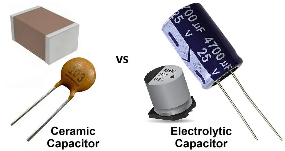
Digital circuits often generate power supply noise due to rapid switching. Placing decoupling capacitors (e.g., 0.1 μF ceramic capacitors) close to the power pins of digital ICs filters out high-frequency noise before it reaches analog components. Use multiple capacitors in parallel for different frequency ranges if needed.
The substrate’s dielectric properties can affect capacitor performance at high frequencies, so choose a material with low parasitic effects to ensure effective noise suppression.
2. Minimize Loop Areas in Signal Paths
Large loop areas in signal traces or ground returns act as antennas, picking up or radiating noise. Keep signal traces short and direct, especially for high-speed digital lines, and ensure return paths are as close as possible to the signal path. This is particularly important in mixed-signal designs where noise from digital loops can couple into analog circuits.
A substrate with a low dielectric constant can help reduce parasitic capacitance in tightly packed designs, further minimizing loop-related noise.
3. Shielding Sensitive Analog Areas
For extremely sensitive analog circuits, consider adding shielding on the PCB. This can be achieved by surrounding critical analog components with grounded copper pours or by using metal cans over specific areas. The substrate should support these shielding structures without introducing additional noise paths.
Grounding Techniques for Mixed-Signal PCBs
Grounding is the backbone of noise reduction in mixed-signal designs. A poorly designed ground system can undo all the benefits of a carefully chosen substrate. Let’s explore effective grounding techniques.
1. Single-Point Grounding
As mentioned earlier, connecting analog and digital ground planes at a single point prevents ground loops while maintaining a common reference. This point should be near the power supply input to minimize voltage differences across the board.
The substrate’s role here is to ensure uniform conductivity across the ground plane. Materials with inconsistent dielectric properties can cause uneven current distribution, leading to noise.
2. Star Grounding for Multiple Components
In designs with multiple analog components, use a star grounding topology. This involves routing all ground connections to a central point rather than daisy-chaining them. Star grounding reduces the chance of noise coupling between components, especially in low-frequency analog circuits.
Ensure the substrate supports a solid ground plane beneath the star point to handle return currents effectively.
3. Avoid Ground Plane Cuts Under High-Speed Traces
Cuts or splits in the ground plane under high-speed digital traces can disrupt return paths, leading to noise and signal integrity issues. If a split is necessary for isolation, route traces to avoid crossing the split or use stitching vias to maintain a continuous return path.
Common Substrate Materials for Mixed-Signal PCBs
Let’s review some widely used substrate materials and their suitability for mixed-signal designs. Each material has trade-offs in terms of cost, performance, and availability.
- FR-4: A cost-effective option with a dielectric constant of around 4.5 and a loss tangent of 0.02. Suitable for low to mid-frequency mixed-signal designs (up to 1 GHz). However, it may not perform well for high-speed digital or ultra-sensitive analog applications due to higher signal loss.
- High-Frequency Laminates: Materials like Rogers RO4350B offer a lower dielectric constant (around 3.48) and loss tangent (0.0037), making them ideal for high-frequency digital and analog circuits. These are more expensive but provide excellent signal integrity.
- Polyimide: Used in flexible or high-temperature applications, polyimide substrates have a Dk of about 3.5 and good thermal stability. They’re less common in rigid mixed-signal PCBs but useful for specific niche designs.
Selecting a substrate often involves balancing performance with budget constraints. For most mixed-signal projects, starting with FR-4 and upgrading to high-frequency materials for critical sections is a practical approach.
Conclusion: Making the Right Choice for Your Mixed-Signal PCB
Selecting the right PCB substrate for mixed-technology assembly is a complex but crucial task. By understanding the needs of both analog and digital circuits, you can choose a material that supports signal integrity, reduces noise, and ensures reliable performance. Focus on dielectric properties, loss tangent, and thermal conductivity while implementing isolation and grounding techniques to address interference challenges.
Whether you’re working on a low-frequency sensor system or a high-speed communication device, the substrate sets the foundation for success. Combine careful material selection with strategic design practices like split ground planes, decoupling capacitors, and star grounding to create robust mixed-signal PCBs. With these insights, you’re well-equipped to tackle the unique demands of mixed-technology assemblies and deliver high-quality designs.
 ALLPCB


