ALLPCB


Introduction
This article examines the consequences of adding reset inputs to FPGA designs and reviews basic considerations for encoding functionality using reset signals. Designers may overlook the effects of using resets, but incorrect reset strategies can incur significant penalties. Reset functionality can negatively affect an FPGA design's speed, area, and power.
FPGA primitives and available features
Before proceeding, it is important to emphasize a basic principle: an FPGA is a programmable device, but not every function inside an FPGA can be arbitrarily modified. That principle is illustrated throughout this article.
Figure 1 shows the D-type flip-flop (DFF) provided in Xilinx 7-series FPGAs.
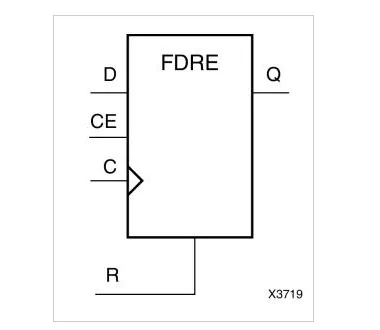
This particular DFF has a synchronous reset (R) and a clock enable (CE) input. In Xilinx documentation it is called FDRE (flip-flop, D, synchronous reset, with clock enable). Its truth table is shown in Figure 2.
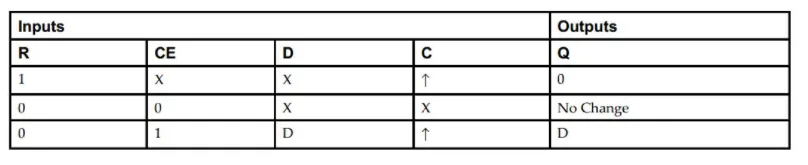
R, CE, D and C are the DFF inputs: reset, clock enable, data input and clock, respectively. X denotes "don't care" and ↑ denotes the rising clock edge. The reset is synchronous because it only takes effect on the clock rising edge.
The DFF is a design element used as a building block for larger designs. It can be used to register required signals, and its reset and clock-enable inputs are available for use as needed.
You can choose whether to use the available features of a building block, but you cannot add unsupported features to a given primitive. For example, the FDRE element only supports synchronous reset. If both asynchronous and synchronous resets are needed, FDRE cannot implement that directly. In that case the synthesis tool must use other resources or combine available primitives to implement the desired behavior. FPGA low-level primitives are fixed, but once configured they can be connected to build larger functions.
As a subtler example of how FPGA granularity affects implementation: according to the FDRE truth table the reset (R) input has higher priority than the clock enable (CE) input (rows indicate CE is "don't care" when R is 1). If HDL code describes a DFF with both reset and clock-enable but assigns CE a higher priority than R, the synthesis tool must use resources other than FDRE or combine primitives to implement that behavior. See the relevant Xilinx white paper for details.
These examples show that to achieve efficient designs you must study FPGA primitives the same way you study discrete device datasheets. The following sections provide additional examples of that principle.
Shift register LUTs (SRL)
Xilinx synthesis tools can implement LUT-based shift registers that are denser and faster than cascaded DFFs. These efficient shift registers, called SRLs, do not support reset inputs. Therefore, if a shift register does not truly require a reset, avoid describing a reset so the synthesis tool can infer an SRL-based implementation. If RTL describes a shift register with reset, the tool will implement it with DFFs, or add extra logic around an SRL to provide reset behavior. SRLs are inferred from simple shift constructs in HDL.
Block RAM
Similarly, Block RAM contents cannot be explicitly reset via a reset input. For this reason, avoid using resets when mapping behavior to Block RAM. More details can be found in vendor documentation.
Multipliers and other specialized resources
Unlike SRLs or Block RAM, some modules such as multipliers impose restrictions on reset types; they only support synchronous reset. Replacing an asynchronous reset strategy with a synchronous one for such blocks can significantly improve maximum operating frequency.
In summary, incorrect reset strategies prevent synthesis tools from leveraging FPGA optimized modules, which negatively impacts area, power and speed. The following section shows examples where synthesis uses DFF reset/set ports to optimize implementations.
Using set/reset inputs for implementation optimization
It is generally advisable to avoid set/reset inputs when possible. This helps synthesis tools apply optimizations by examining DFF set/reset inputs to simplify implementations. To illustrate, consider the schematic in Figure 3.
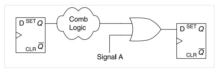
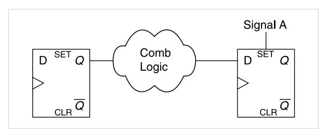
In Figure 3, when "signal A" is asserted, the DFF output goes high on the clock edge regardless of the combinational block's output. Synthesis can eliminate the OR gate and apply "signal A" to the DFF's synchronous set input, as shown in Figure 4. Now when "signal A" is asserted, the DFF will be set high on the clock edge; otherwise the output is determined by the combinational logic. The transformed design provides the required functionality while improving speed and area by removing the OR gate.
Interestingly, synthesis may sometimes perform the inverse transformation and implement the Figure 4 behavior as Figure 3. In Xilinx 7-series, all DFFs in a slice share the same CK, SR (set/reset) and CE signals. That means a DFF with SR connected to "signal A" cannot be in the same slice as a DFF whose SR is connected to a different signal. If control signals (CK, SR and CE) differ, DFFs must be placed in different slices, which can reduce slice utilization for designs with many low-fanout reset signals. Each low-fanout reset may occupy several DFFs in a slice, leaving the remaining DFFs unused. In that case, synthesis may prefer to implement the logic in a form that avoids using the reset input so DFFs can share control signals and be placed in the same slice, increasing resource utilization.
Replacing gates with set/reset usage
In Figures 3 and 4, an OR gate feeding a DFF can be replaced by using the DFF's set input. Similarly, an AND gate can be replaced by using the DFF's reset input, as shown in Figure 5.
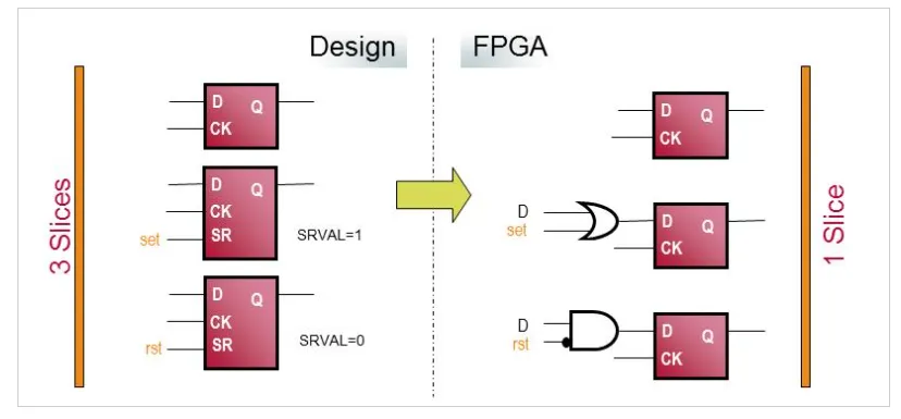
In Figure 5, the SRVAL attribute specifies the DFF output value after asserting the SR input. Thus, for the left-middle DFF the SR input is used as a set, while for the lower-left DFF the SR input functions as a reset. The upper DFF does not use its reset input.
The three left DFFs initially cannot be placed in the same slice due to differing control signals. After the transformations discussed above they share the same control signals and can be placed together in a slice. Note that these transformations do not apply for asynchronous set/reset signals, which is why synchronous set/reset signals are generally recommended over asynchronous ones.