 ALLPCB


When it comes to PCB design, working with mmWave frequencies (typically ranging from 24 to 100 GHz) introduces unique challenges and considerations compared to traditional lower-frequency designs. The key differences lie in the materials used, the precision required in layout, and the management of signal integrity due to the extremely short wavelengths. For engineers and designers working on multilayer PCBs for microwave and higher frequencies, understanding these differences is critical to creating reliable and high-performing circuits. In this blog, we’ll dive deep into what sets mmWave PCB design apart and provide practical insights to help you succeed in this specialized field.
Introduction to mmWave and Its Impact on PCB Design
Millimeter-wave (mmWave) technology is at the forefront of modern applications like 5G networks, automotive radar, IoT devices, and high-speed wireless communication. These systems operate at frequencies far beyond traditional RF ranges, often between 24 GHz and 100 GHz, where wavelengths shrink to mere millimeters. This shift to higher frequencies means that even tiny imperfections in a PCB can lead to significant signal loss, interference, or performance issues.
For multilayer PCBs designed for microwave and higher frequencies, the stakes are even higher. The design must account for tighter tolerances, specialized circuit materials, and advanced manufacturing techniques. Whether you're working on a radar system or a 5G base station, mastering mmWave PCB design starts with understanding what makes it different. Let’s explore the key factors that set mmWave apart from standard PCB design.

Key Differences in mmWave PCB Design
1. Shorter Wavelengths and Tighter Tolerances
At mmWave frequencies, wavelengths are incredibly short—ranging from 10 mm at 30 GHz down to just 3 mm at 100 GHz. This means that the physical dimensions of traces, vias, and other components on a PCB must be extremely precise. A misalignment or variation of even 0.1 mm can cause significant phase shifts or signal degradation. In contrast, lower-frequency designs (below 6 GHz) can tolerate larger deviations without noticeable impact.
For multilayer PCBs, this precision becomes even more critical. Each layer must align perfectly to maintain signal integrity across the stack. Designers often need to work with manufacturing tolerances as tight as ±0.05 mm for trace widths and spacings. This level of accuracy requires advanced design tools and close collaboration with fabrication partners to ensure the final product matches the intended specifications.
2. Material Selection for Higher Frequencies
The choice of circuit materials plays a massive role in mmWave PCB design. Standard FR-4 materials, commonly used in lower-frequency designs, are unsuitable for microwave and higher frequencies due to their high dielectric loss and inconsistent dielectric constant (Dk) at these ranges. Instead, specialized materials with low loss tangents and stable Dk values are essential.
Some key material properties to consider include:
- Dielectric Constant (Dk): A stable Dk (typically between 2.2 and 3.5 for mmWave materials) ensures consistent signal propagation. Variations in Dk can cause impedance mismatches.
- Loss Tangent (Df): A low loss tangent (ideally below 0.003 at 10 GHz) minimizes signal attenuation. For comparison, FR-4 often has a loss tangent of 0.02, which is far too high for mmWave.
- Thermal Stability: mmWave applications often involve high power densities, so materials must withstand temperature fluctuations without degrading.
Popular material families for mmWave designs include PTFE-based laminates and advanced thermoset resins, which offer excellent performance at higher frequencies. Additionally, bonding materials and prepregs used in multilayer structures must also be chosen carefully to minimize loss and maintain layer-to-layer consistency.
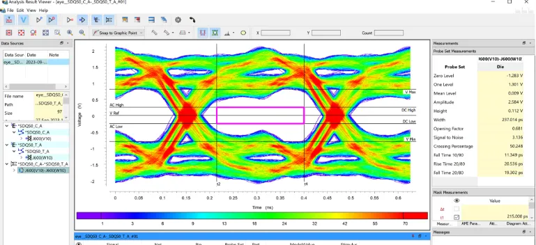
3. Signal Integrity Challenges in Multilayer Designs
Signal integrity is a major concern in mmWave PCB design, especially for multilayer boards. At higher frequencies, signals are more susceptible to losses caused by skin effect, dielectric absorption, and crosstalk. Here are some specific challenges and solutions:
- Skin Effect: At mmWave frequencies, current flows primarily on the surface of conductors, increasing resistance. To combat this, designers use smoother copper finishes and wider traces where possible.
- Crosstalk: With shorter wavelengths, even small spacings between traces can lead to interference. Maintaining a minimum spacing of at least 3 times the trace width can help reduce crosstalk in multilayer layouts.
- Impedance Control: Achieving a consistent 50-ohm impedance (common for RF designs) requires precise control of trace dimensions and dielectric thickness. For example, a trace width of 0.15 mm on a 0.127 mm thick substrate might be needed to achieve the desired impedance at 28 GHz.
Designers often use simulation tools to model signal behavior before fabrication, ensuring that potential issues are identified and addressed early in the process.
4. Thermal Management at Higher Frequencies
mmWave circuits often generate significant heat due to high power densities and the compact nature of multilayer designs. Poor thermal management can lead to performance degradation or even component failure. To address this, designers must incorporate thermal vias, heat sinks, and materials with high thermal conductivity into their PCBs.
For instance, placing thermal vias under high-power components can help dissipate heat through the multilayer stack to a ground plane or external heat sink. Additionally, selecting materials with thermal conductivity values above 0.5 W/m·K can improve heat distribution across the board.
Design Tips for mmWave Multilayer PCBs
Creating a successful mmWave PCB design requires careful planning and attention to detail. Below are actionable tips to guide you through the process of designing multilayer boards for microwave and higher frequencies.
1. Optimize Layer Stackup for Signal Integrity
In multilayer PCBs, the layer stackup directly impacts signal performance. Place high-frequency signal layers close to ground planes to minimize interference and maintain controlled impedance. For example, a common stackup for a 6-layer mmWave PCB might include:
- Layer 1: Signal (mmWave traces)
- Layer 2: Ground Plane
- Layer 3: Power Plane
- Layer 4: Ground Plane
- Layer 5: Signal (control lines)
- Layer 6: Ground Plane
This configuration helps shield sensitive mmWave signals from noise while providing stable reference planes for impedance control.
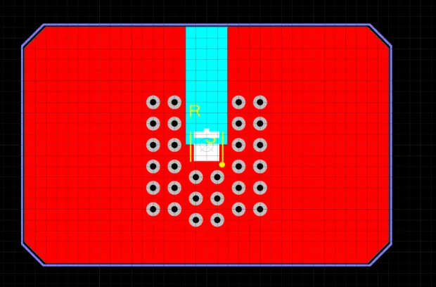
2. Minimize Via Usage and Optimize Transitions
Vias introduce parasitic inductance and capacitance, which can disrupt signals at mmWave frequencies. Use vias sparingly and opt for blind or buried vias in multilayer designs to reduce their impact. When vias are necessary, ensure smooth transitions by matching their impedance to the trace (often around 50 ohms) and using back-drilling to remove unused via stubs.
3. Use Advanced Simulation Tools
Simulation is a must for mmWave PCB design. Tools that support electromagnetic (EM) analysis can predict signal behavior, identify potential crosstalk, and optimize impedance matching. Running simulations early in the design phase can save time and costly revisions during fabrication.
4. Collaborate with Fabrication Experts
mmWave designs often push the limits of manufacturing capabilities. Work closely with your fabrication team to confirm that your design aligns with their tolerances and material options. For instance, some processes may struggle to achieve trace widths below 0.1 mm or maintain dielectric thicknesses within ±0.02 mm. Early collaboration ensures that your design is manufacturable without compromising performance.
Common Applications of mmWave PCBs
Understanding where mmWave PCBs are used can provide context for their design requirements. Here are some of the most common applications:
- 5G Communication: mmWave frequencies (like 28 GHz and 39 GHz) enable ultra-fast data rates for 5G networks, requiring multilayer PCBs with low-loss materials and precise layouts.
- Automotive Radar: Advanced driver-assistance systems (ADAS) rely on mmWave radar operating at 77 GHz for object detection, demanding high-performance circuit materials.
- IoT and Wireless Connectivity: High-frequency mmWave PCBs support short-range, high-speed connections in smart devices and industrial systems.
Each of these applications underscores the need for specialized design practices to handle the challenges of higher frequencies and multilayer configurations.
Conclusion: Mastering mmWave PCB Design
Designing PCBs for mmWave frequencies is a complex but rewarding endeavor. The transition to higher frequencies introduces challenges like shorter wavelengths, stricter tolerances, and the need for specialized circuit materials. However, by focusing on precise layouts, selecting the right materials for microwave applications, and leveraging advanced tools, engineers can create multilayer PCBs that deliver exceptional performance.
At the core of successful mmWave design is a deep understanding of how these factors interplay in multilayer structures. Whether you’re working on a 5G antenna or an automotive radar system, the principles outlined in this blog can guide you toward better designs. Keep refining your skills, stay updated on material advancements, and collaborate with fabrication experts to ensure your PCBs meet the demands of tomorrow’s technologies.


