 ALLPCB


Are you new to electronics and wondering how to create your first printed circuit board (PCB)? PCB design might seem intimidating at first, but with the right guidance, tools, and steps, it’s a skill you can master. In this comprehensive guide, we’ll walk you through the entire process of designing a PCB, from creating a schematic to soldering components. Whether you're searching for easy PCB design software for beginners, a PCB layout tutorial for newbies, or tips on soldering components on a PCB, this step-by-step tutorial will help you get started. Let’s dive into the world of PCB design and turn your ideas into reality with ALLPCB!
Why Learn PCB Design as a Beginner?
PCBs are the backbone of modern electronics, found in everything from smartphones to home appliances. Designing your own PCB allows you to customize circuits, save space compared to breadboards, and create reliable, professional-grade projects. For beginners, learning PCB design opens doors to endless possibilities in electronics, whether you’re a hobbyist or aspiring engineer. Plus, with affordable manufacturing options and user-friendly tools available today, there’s no better time to start.
In this guide, we’ll cover every stage of the process, ensuring you have the knowledge and confidence to build your first board. We’ll also touch on resources like PCB design online courses to further your learning.
Step 1: Understanding the Basics of PCB Design
Before jumping into design software, let’s cover the fundamentals. A PCB is a board that connects electronic components using conductive tracks, pads, and other features. It replaces messy wiring with a neat, organized layout. As a beginner, your goal is to design a board that functions correctly and can be manufactured easily.
Key terms to know:
- Schematic: A diagram showing how components connect electrically.
- Layout: The physical arrangement of components and traces on the board.
- Traces: Copper paths that act as wires to connect components.
- Vias: Small holes that connect traces between different layers of the board.
Start with a simple project, like a basic LED circuit, to practice these concepts. This will help you understand how schematics translate into physical layouts.
Step 2: Gathering the Right Tools for PCB Design
One of the first hurdles for beginners is choosing the right tools. Thankfully, there are plenty of easy PCB design software for beginners that simplify the process. Look for free or low-cost programs with intuitive interfaces and plenty of tutorials. These tools often include libraries of components and templates to help you start designing quickly.
Besides software, you’ll need:
- A computer: Ensure it meets the software’s system requirements.
- Basic components: Resistors, capacitors, LEDs, and a microcontroller if needed.
- Soldering kit: For assembling your board later (more on this in Step 6).
ALLPCB supports hobbyists and professionals by offering resources and services to help turn your designs into physical boards. Explore our platform for affordable manufacturing once your design is ready.
Related Reading: Top 10 PCB Design Software Tools for Engineers in 2025
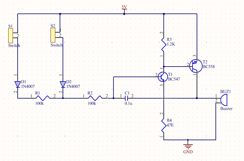
Step 3: Creating a PCB Schematic
The first major step in PCB design is creating a PCB schematic. This is like a blueprint for your circuit, showing how each component connects electrically. Think of it as planning before building. Here’s how to do it:
- Define Your Circuit: Decide what your PCB will do. For example, a simple circuit to blink an LED might include a microcontroller, resistor, and LED.
- Choose Components: Select components based on their specifications, like a resistor with a value of 220 ohms for an LED circuit to limit current.
- Draw Connections: Use your design software to place components and draw wires between them. Ensure positive and negative terminals are connected correctly.
- Label Everything: Add labels to components (e.g., R1 for a resistor) and nets (connection points) to keep your schematic organized.
- Check for Errors: Most software has a feature to detect unconnected pins or incorrect wiring. Fix any issues before moving on.
A well-organized schematic makes the next step—layout design—much easier. Take your time here to avoid mistakes later.
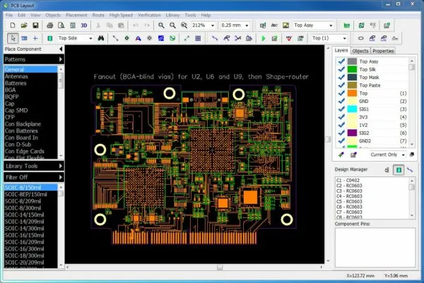
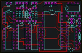
Step 4: Designing the PCB Layout (Tutorial for Newbies)
Now that your schematic is ready, it’s time to design the physical layout of your board. This PCB layout tutorial for newbies will guide you through the process of turning your schematic into a manufacturable design.
- Import the Schematic: Most design tools let you import your schematic directly into the layout editor. This brings over all components and connections.
- Place Components: Arrange components on the board. Keep related parts close together to minimize trace lengths. For example, place a decoupling capacitor (typically 0.1 μF) near a microcontroller’s power pin to reduce noise.
- Route Traces: Draw copper traces to connect components based on the schematic. Aim for short, direct paths to avoid signal interference. For power traces, use wider paths (e.g., 20-30 mils for low-current designs) to handle current safely.
- Add a Ground Plane: A ground plane is a large copper area connected to ground. It reduces electrical noise, especially in analog circuits, and improves signal integrity.
- Check Design Rules: Use the software’s design rule check (DRC) to ensure your layout meets manufacturing standards, like minimum trace width (often 6-8 mils for basic designs) and spacing.
Common beginner mistakes include placing components too close together, which can make soldering difficult, or forgetting to include a ground plane. Double-check your layout to avoid these issues.
Related Reading: High-Speed FR-4 PCB Design: Techniques for Signal Integrity
Step 5: Exporting and Manufacturing Your PCB
Once your layout is complete, it’s time to prepare your design for manufacturing. This step involves generating files that a manufacturer can use to produce your board.
- Generate Gerber Files: These are standard files that describe your PCB’s layers, traces, and drill holes. Most design software has an option to export Gerber files.
- Review Your Files: Use a free Gerber viewer to ensure everything looks correct before sending them to a manufacturer.
- Choose a Manufacturer: With ALLPCB, you can upload your files directly to our platform for quick, affordable production. We offer fast turnaround times and support for beginners.
- Order Your PCB: Specify details like board thickness (commonly 1.6mm for standard designs) and copper weight (1 oz is typical for hobbyist projects). Place your order and wait for delivery.
Starting with a small batch (e.g., 5-10 boards) is a good idea for beginners. This way, you can test your design without a large upfront cost.
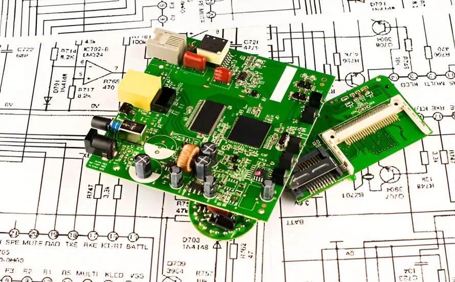
Step 6: Soldering Components on a PCB
Once your PCB arrives, it’s time to assemble it by soldering components on a PCB. Soldering is the process of attaching components to the board using a heated metal alloy called solder. Here’s how to do it safely and effectively:
- Prepare Your Workspace: Work in a well-ventilated area with a soldering iron (25-40 watts for beginners), solder wire (lead-free, 0.5-1mm diameter), and a soldering stand. Wear safety glasses to protect your eyes.
- Insert Components: Place components into their designated holes or pads on the PCB. Bend the leads slightly on through-hole components to hold them in place.
- Heat the Joint: Touch the soldering iron tip to the pad and component lead for 2-3 seconds to heat them. Then, apply solder to the joint (not the iron tip) until it flows smoothly around the connection.
- Trim Excess Leads: For through-hole components, use wire cutters to trim excess leads after soldering.
- Inspect Your Work: Look for shiny, smooth solder joints. Dull or cracked joints may indicate a “cold solder joint,” which can cause poor connections. Reheat and add more solder if needed.
Practice on a scrap board first if you’re new to soldering. It takes patience, but you’ll improve with each attempt. Avoid overheating components, as it can damage them—limit soldering time to 5 seconds per joint.
Step 7: Testing and Troubleshooting Your PCB
After soldering, test your PCB to ensure it works as intended. Use a multimeter to check for continuity between connections and verify voltages at key points. For example, in a simple LED circuit, confirm that 5V (or your expected voltage) is present at the microcontroller’s power pin.
If something doesn’t work, troubleshoot by:
- Checking solder joints for cracks or poor connections.
- Verifying component placement—did you install anything backward?
- Reviewing your schematic and layout for design errors.
Fix issues one at a time, testing after each change. This methodical approach helps isolate problems.
Step 8: Learning More with PCB Design Online Courses
Designing your first PCB is just the beginning. To deepen your skills, consider enrolling in PCB design online courses. These courses cover advanced topics like high-speed design, multi-layer boards, and electromagnetic interference (EMI) reduction. Many platforms offer free or affordable courses tailored for beginners, often with hands-on projects to reinforce learning.
Look for courses that teach:
- Signal integrity for faster circuits (e.g., managing impedance, often around 50 ohms for RF designs).
- Thermal management to prevent overheating.
- Designing for manufacturability to reduce costs.
Continuous learning will help you tackle more complex projects over time. ALLPCB also provides resources and support to guide you as you grow in your PCB design journey.
Tips for Success in PCB Design
As a beginner, keep these tips in mind to make your PCB design experience smoother:
- Start Small: Begin with simple circuits to build confidence before moving to complex designs.
- Double-Check Everything: Errors in schematics or layouts can be costly. Review your work at every stage.
- Learn from Mistakes: Your first PCB might not be perfect, and that’s okay. Each project teaches you something new.
- Use Community Resources: Online forums and communities are great places to ask for advice and share your progress.
Conclusion: Bring Your PCB Designs to Life with ALLPCB
Designing your first PCB is an exciting milestone in your electronics journey. By following this step-by-step guide, you’ve learned how to create a schematic, design a layout, manufacture a board, and assemble it with soldered components. With easy PCB design software for beginners, actionable tutorials like this PCB layout tutorial for newbies, and resources such as PCB design online courses, you’re well on your way to mastering this skill.
ALLPCB is here to support you every step of the way. Our platform makes it simple to turn your designs into high-quality boards with fast delivery and affordable pricing. Start small, experiment with new ideas, and watch your skills grow. Upload your first design to ALLPCB today and see your creation come to life!


