ALLPCB


As semiconductor technology advances, design engineers face increasing complexity at every stage of the development process. Chip designers must ensure accurate integrated circuit (IC) logic, performance, power efficiency, and yield on silicon. System developers extend these challenges to board-level reference designs, boot code, operating system (OS) ports, and application software, alongside flash programming, manufacturing test methods, and field support. Meeting tight deadlines and cost targets remains a significant challenge.
Evolving Debugging Challenges
The nature of system testing and debugging evolves with advancements in hardware and software development. Moore's Law impacts not only processor and memory design but also the integration of system functions, operating systems (or real-time operating systems), and the growing volume of application software in embedded systems. In the era of large-scale integration (LSI) components, with at least 1,000 gates, central processing units (CPUs) were limited by semiconductor process technology, power consumption, and yield. Debugging focused on integrating hardware functions, adjusting inter-chip timing, and verifying logic functionality. System software was constrained to a few hundred kilobytes due to limited memory.
Today, memory capacity and CPU clock frequencies have significantly increased. Debugging and testing challenges have shifted from hardware component integration to system hardware simulation before system-on-chip (SoC) fabrication, system software modeling, and integration of hundreds of megabytes of system software. Modern embedded devices typically require a full-featured embedded operating system, running multiple applications managed by a memory management unit (MMU), and increasingly include network functionality, such as local area network (LAN) or wireless connectivity for control, database access, or voice, data, and video services.
Contemporary embedded solutions feature SoCs with millions of gates, integrating cache, scratchpad random-access memory (RAM), and peripheral functions on a single chip. Many component interfaces are now embedded within the chip, no longer accessible via pins or board-level testing, and CPU cores operate at hundreds of megahertz with integrated hardware interfaces, rendering traditional testing methods obsolete.
JTAG and Boundary-Scan Testing
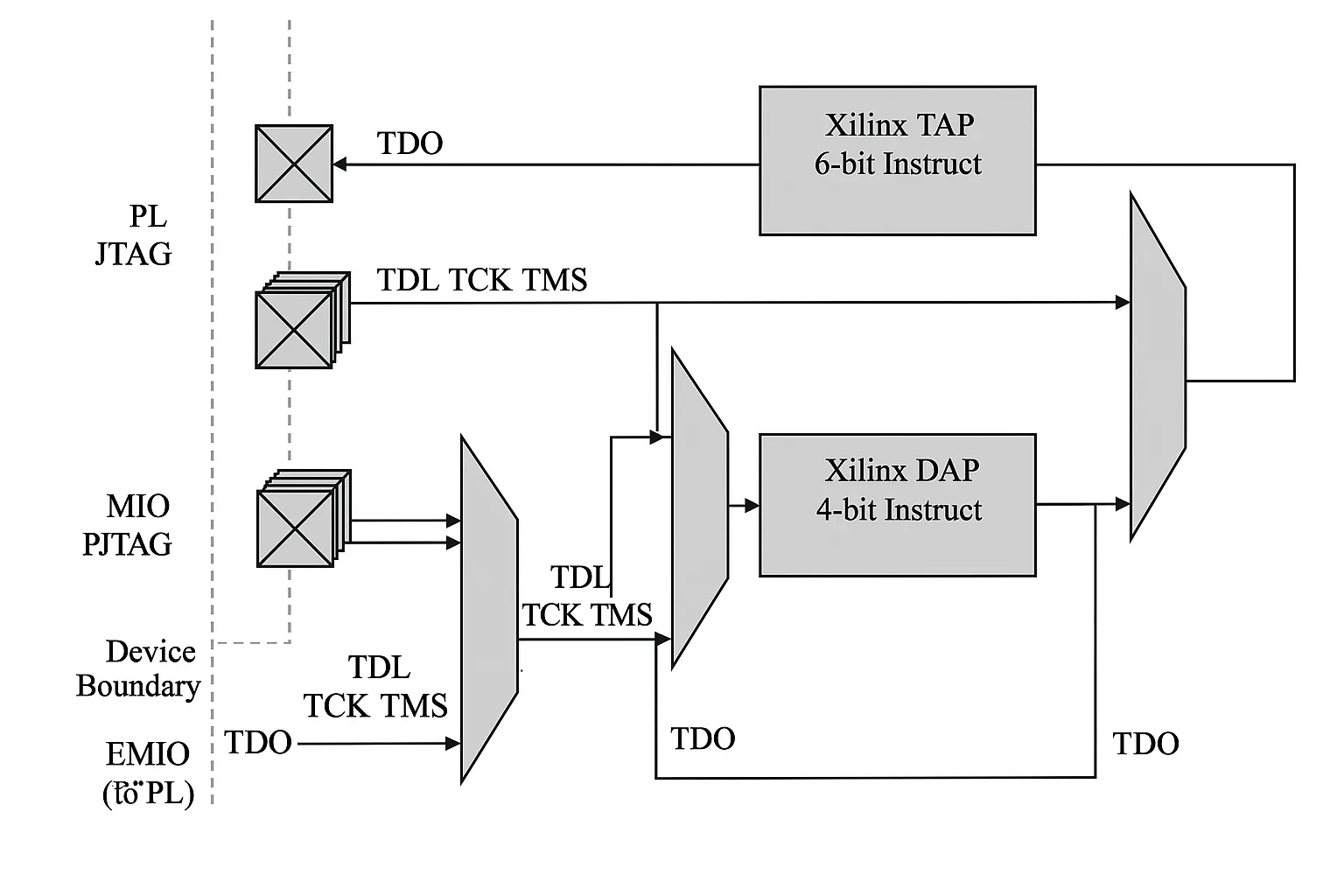
The Joint Test Action Group (JTAG) standard, formalized as IEEE 1149.1, introduced a serial scan chain method in the 1990s to address board-level testing challenges. By incorporating additional shift registers into the I/O paths of each IC, JTAG enables boundary-scan testing. Before this approach, debugging solder joint issues beneath chip components was difficult. Each IC was tested for functionality before board assembly, so failures in assembled printed circuit boards (PCBs) were attributed to solder bridges, gaps, or defects. Boundary-scan testing resolves this by providing a serial scan path through I/O registers, executed by complex test programs tailored to each board to identify faulty chips or devices for rework or replacement.
The JTAG method allows testing of complex systems with minimal pin count, requiring only five pins for the test access port: Test Reset (TRST), Test Clock (TCK), Test Data Input (TDI), Test Data Output (TDO), and Test Mode Select (TMS). These pins facilitate resetting JTAG logic, setting scan rates, and managing serial data input/output and mode selection.
JTAG for CPU Core Debugging
With CPU cores now integrating cache, on-chip buses, MMUs, and peripherals, JTAG provides direct access to internal debugging logic. As cache and peripherals are embedded within the chip, debugging logic must also reside on-chip. Host-based debugger software can assert debug exceptions, redirecting the processor to execute instructions from debug logic registers, enabling operations such as:
- Run-control: Start, stop, single-step, and step into/over (source or instruction).
- Setting hardware and software breakpoints.
- Specifying conditions or scripts to execute at breakpoints.
- Controlling system reset and initialization.
- Debugging or programming code into flash memory.
- Executing flash programming and other semi-hosted utilities.
In both boundary-scan and software debugging applications, JTAG serves as the physical layer communication interface, akin to the PHY layer in the ISO Open Systems Interconnection model. Supported debugging protocols are implemented in the CPU core's debug logic and host-based debugger software.
Advantages of JTAG Debugging
Using a debugger with JTAG access offers several benefits:
- Direct access to otherwise hidden CPU cores.
- No use of system I/O ports (e.g., serial or Ethernet).
- Minimal or no system memory allocation, unlike monitor-based debugging.
- No risk of monitor crashes during system failures.
- No dependency on target system power (except for some USB-only probes).
- Ability to read registers/memory without halting the CPU, if supported by debug logic.
- System reset or initialization during debugging sessions.
- Non-intrusive connection to debug logic.
Limitations of JTAG Debugging
JTAG debugging has limitations:
- Not ideal for transferring large programs (>20 MB), especially for systems with 10/100BaseT Ethernet access.
- Multi-core debugging requires additional on-chip hardware for synchronized operations, as asynchronous JTAG commands may introduce delays of hundreds of CPU cycles.
- Traditional methods like "printf" remain useful for extracting debug states.
Trace Functionality and On-Chip Buffers
Not all debugging functions rely on the JTAG scan chain. Some processors support trace collection, which tracks execution through branches and interrupts, saving significant debugging time. Early implementations, like ARM's Embedded Trace Macrocell (ETM) and MIPS' EJTAG PCTrace, used JTAG to set operation modes but relied on separate parallel buses and protocols for trace data offloading, requiring additional pins and increasing probe costs.
Advanced trace techniques use on-chip trace buffers to collect program execution data at CPU clock rates. This approach reduces costs by uploading trace data through the same JTAG scan chain used for run-control debugging. ARM's Embedded Trace Buffer (ETB) and MIPS' PDTrace with Trace Control Block (TCB) provide comprehensive trace information, though at the cost of increased chip area. Intel XScale processors collect branch and count data in smaller on-chip buffers, enabling execution flow reconstruction without real-time markers. The amount of trace data depends on buffer size, requiring trade-offs between cost and debugging needs.