ALLPCB


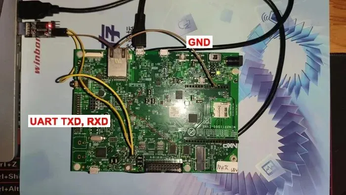
When connecting an RW612 board to an RT1060 board via UART, the RT1060 fails to boot if the RW612 board is powered on first. This is a typical power-up sequencing issue in the i.MX RT series. This article will analyze the root cause of this failure.
Note: This article uses the i.MXRT1060 as an example, but the principles apply to other MCUs in the i.MXRT1xxx series.
1. Reproducing the Issue
The issue can be reproduced without a second MCU board by using a 3.3V USB-to-serial module connected to the i.MXRT1060's ROM ISP UART port.
The TXD and RXD pins of the USB-to-serial module used for this test have different drive strengths. The open-circuit voltage for both is 3.55V. However, when connected to an unpowered RT1060-EVKB, this voltage drops. The following table shows the boot results for an RT1060 board under various connection scenarios with the USB-to-serial module continuously powered.
| Module TXD Chip GPIO_AD_B0_13 |
Module RXD Chip GPIO_AD_B0_12 |
NVCC_GPIO | NVCC_SD1 | NVCC_EMC | NVCC_SD0 | DCDC_PSWITCH | DCDC_IN | DCDC_LP | VDD_SOC_IN | Boot Result |
|---|---|---|---|---|---|---|---|
| Not Connected | Not Connected | 0V | 0V | 0V | 0V | 1.275V | Success |
| Not Connected | Connected (0.83V) | 0.33V | 0V | 0.33V | 0.33V | 1.275V | Success |
| Connected (2.22V) | Not Connected | 1.42V | 0V | 1.42V | 1.42V | 0V | Failure |
| Connected (2.24V) | Connected (1.79V) | 1.46V | 0V | 1.46V | 1.46V | 0V | Failure |
The test results show that the RT1060 fails to boot primarily because there is no voltage on VDD_SOC_IN after power-up, indicating the internal DCDC converter has not started.
2. Internal DCDC Power-Up Sequence Requirements
To understand the failure, it's necessary to review the internal DCDC module of the i.MXRT1xxx series. In cost-sensitive applications, using the internal DCDC converter to power the core is a common approach. Therefore, the successful startup of this module is critical for the core's operation.
The NXP document "i.MX RT Hardware Development Guide for the MIMXRT1050/MIMXRT1060 Processor" specifies strict power-up sequencing requirements. A common point of failure is not meeting the minimum 1 ms delay between DCDC_IN becoming stable (at 3.0V) and DCDC_PSWITCH reaching 1.5V. If this requirement is not met, the internal DCDC module may fail to start, resulting in no output voltage for the core (at the DCDC_LP pin).
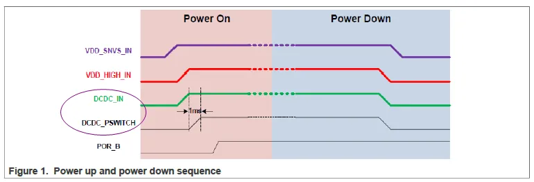
- The VDD_SNVS_IN supply must be turned on before any other power supply or connected (shorted) with the VDD_HIGH_IN supply.
- If a coin-cell battery is used to power VDD_SNVS_IN, ensure that it is connected before any other supply is switched on.
- An RC delay circuit is recommended for providing the delay between DCDC_IN stable and DCDC_PSWITCH. The total RC delay should be 5-15 ms.
- DCDC_IN must reach a minimum 3.0 V within 0.3 x RC.
- The delay from DCDC_IN stable at 3.0 V min to DCDC_PSWITCH reaching 0.5 x DCDC_IN (1.5 V) must be at least 1 ms.
- The power-up slew rate specification for other power domains is 360 V/s - 36k V/s.
- POR_B must be held low during the entire power up sequence.
3. Impact of Early GPIO Power-Up
Examining the RT1060-EVKB schematic, the external 3.3V input (DCDC_3V3) supplies NVCC_GPIO, NVCC_SD1, NVCC_EMC, and DCDC_IN. Additionally, DCDC_IN feeds DCDC_PSWITCH through an RC delay circuit, which complies with the hardware design guidelines.

On the RT1060, the GPIO_AD_Bx and GPIO_Bx pad groups are both powered by NVCC_GPIO. If any of these GPIO pins receive voltage before the board is powered, this voltage can leak back to the NVCC_GPIO rail. When the USB-to-serial module is connected to the ROM ISP UART pins beforehand, leakage current flows to NVCC_GPIO, then to DCDC_3V3, DCDC_IN, and finally to DCDC_PSWITCH. This effectively pre-charges the capacitor in the DCDC_PSWITCH RC circuit, shortening the time it takes to reach 1.5V when the board is formally powered on. This explains the results in the table: a pre-charge to 0.33V on DCDC_PSWITCH does not violate the timing, but a pre-charge to 1.42V does, as the delay becomes less than 1 ms.
Based on the RT1060-EVKB's power circuit design, applying power early to any GPIO in the NVCC_GPIO, NVCC_SD1, or NVCC_EMC power domains will have the same effect. However, GPIOs powered by NVCC_SD0 will not affect the startup because there is no electrical path between this rail and the DCDC_PSWITCH pin.
4. Solutions for Multi-Board Connections
When encountering this type of issue, the first step should be to measure the voltage on the i.MXRT1xxx's internal DCDC output (DCDC_LP). If it is 0V, a power-up sequencing problem is the likely cause. To avoid this issue when connecting to an RT1060-EVKB, consider the following three methods:
- Add series isolation resistors (e.g., 1 kΩ) to the UART signal lines between the two boards. This will reduce the leakage voltage to NVCC_GPIO. The effectiveness should be verified by measurement.
- Use GPIOs from a power domain that does not interfere with the DCDC_PSWITCH signal. For the RT1060-EVKB, this would be the GPIO_SD_B0_xx pins.
- Redesign the RT1060-EVKB board to use an external PMIC for power, disabling the main chip's internal DCDC converter.