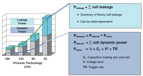
ALLPCB


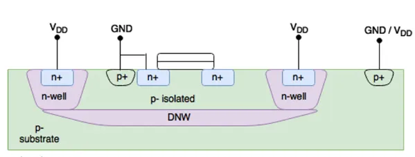
N-well
N-well concept
If a silicon wafer used to fabricate integrated circuits is doped with donor impurities such as phosphorus, the silicon is n-type; if doped with acceptors such as boron, it is p-type. In CMOS processes, NMOS transistors are fabricated directly in a p-type substrate; PMOS transistors are fabricated in an N-well.
Some CMOS processes grow an epitaxial layer on the wafer before device fabrication to reduce latch-up. The epitaxial layer and the original substrate are commonly both referred to as the substrate. A process that uses a p-type substrate with N-wells is called an N-well process. A process that uses an n-type substrate with P-wells is called a P-well process. Modern processes typically favor N-well processes to optimize NMOS performance at the expense of PMOS performance; processes that use both N- and P-wells are called twin-well processes. The N-well and the p-type substrate form a parasitic diode; in CMOS circuits the substrate is usually connected to the lowest potential to keep that diode reverse biased.
Functions of the N-well
Main functions: provide the region for PMOS fabrication; due to relatively low doping concentration, an N-well has higher resistivity and can be used as a well resistor; the N-well and substrate can form a parasitic PNP transistor.
N-well fabrication
After photoresist is applied, the N-well mask is used. The wafer is exposed to light and developed so that the exposed photoresist is removed. An oxide layer is grown as required.
Exposure
In positive photoresist, the exposed areas are dissolved during development and the unexposed areas remain; the photomask acts like an opaque plate where dark areas block light and clear areas transmit it.
In negative photoresist, the exposed areas remain after development while the unexposed areas are removed; the photomask in this case is like a clear plate where opaque areas block light.
In either case the objective is to define a region for doping. During doping, the wafer is exposed to donor atoms; the photoresist blocks implantation except through the openings, allowing dopants to diffuse into the exposed silicon regions.
After removing the photoresist, the N-well is formed. With sufficient diffusion time the N-well reaches the target depth. Donor impurities diffuse both vertically and laterally, so lateral diffusion affects the final N-well geometry and must be considered in layout design rules.
Active Area (Thin Oxide Region)
Active area concept
Source, drain and channel regions together form the transistor active area. Areas outside the active region are field oxide regions (Fox). Active area plus field oxide equals the chip surface: Active + Fox = Surface. The active area is also called Active, diff or thin oxide. Active regions are used to form n-type and p-type devices and to provide contacts to metal1 and to substrate or wells. The active mask mainly opens windows for ion implantation and is used to define regions for local oxidation of silicon (LOCOS) and thin oxide (thin oxide inside enclosed shapes, LOCOS outside).
Active area fabrication
LOCOS (Local Oxidation of Silicon) is a traditional isolation technique in CMOS. A silicon nitride mask enables selective oxidation of silicon, forming a thick field oxide over non-active, heavily doped areas for isolation. LOCOS has drawbacks: field oxide encroachment from the active region (the bird's beak effect) and lateral diffusion of the field, which reduce the actual channel width compared to the drawn layout. For technology nodes below roughly 0.25 um, LOCOS is generally replaced by shallow trench isolation (STI).
Polycrystalline Silicon 1 (Poly1)
Function
Poly1 is primarily used to form MOSFET gates. Poly1 and Poly2 can form a PIP capacitor (poly1 - dielectric - poly2). Poly is also used for poly resistors and poly interconnects, though poly interconnects have relatively high sheet resistance.
Gate formation
Gate formation is a critical process step because it includes growth of the thin gate oxide and deposition and patterning of the poly gate, with the poly gate width often being one of the most critical linewidths on the die. Typical sequence: grow gate oxide > deposit poly > pattern poly mask > etch poly gate.
When poly crosses the active area, source, drain and channel align to the gate (self-aligned process). When not forming devices, poly must not cross active areas to avoid forming parasitic devices. During device formation, poly must extend beyond the edge of the active area to ensure source and drain do not short.
P+/N+ Diffusion Regions
The active area mask opens windows for ion implantation. P+ and N+ diffusion regions enable implantation to set the local doping types. The poly gate can act as a self-aligned mask for NMOS and PMOS source/drain implantation. Implant steps can be performed in any order; N-type source/drain implants can be done first or P-type first.
Contact Holes
Contacts provide electrical connections from silicon active regions and poly to the metal layers. A contact ensures a low-resistance electrical interface between silicon or poly and the subsequently deposited metal.
Metal Layers
After silicidation of contact areas, a metal layer (typically aluminum with copper doping in many processes) is deposited. The wafer is coated with photoresist, exposed with a metal mask, and developed to remove unwanted metal and define interconnects.
Vias
Interlayer dielectrics separate metal layers and the first metal layer from silicon. Many small vias in the dielectric provide electrical channels between adjacent metal layers. Vias are typically filled with a conductive material (for example tungsten) to form vertical electrical connections between metal layers.
Simple Inverter Layout Layers
- N-well (TB)
- Active area (TO)
- Poly1 (GT)
- Poly2 blocking layer (IM)
- P+ diffusion
- N+ diffusion
- Contact
- Metal1
- Via
- Metal2