ALLPCB


Overview
There are many classifications of electrostatic models, including the human body model, mechanical model, charged-device models, and others. Questions often arise about how these models are derived and how their parameters are determined.
1. Human Body Capacitance Model
The human body model (Human Body Model, HBM) is used to simulate the effect of human electrostatic discharge on sensitive electronic devices. The human body is one of the main sources of electrostatic hazards.
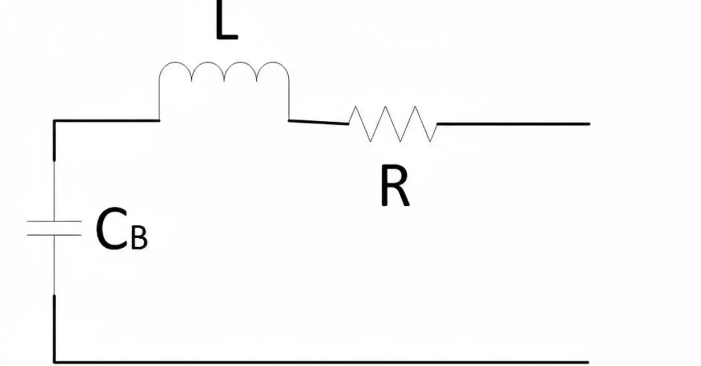
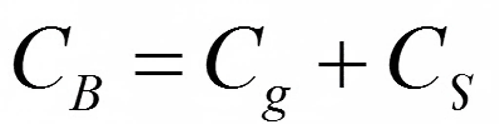
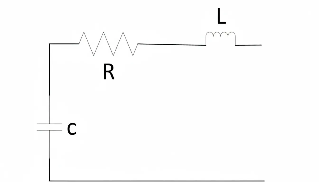
In the equivalent circuit, the resistance R represents the influence of human tissue, moisture, contact resistance, and so on. The inductance L is the body equivalent inductance and is usually negligible. The capacitance C depends on body height, weight, clothing, and surrounding materials; body capacitance has the largest influence.
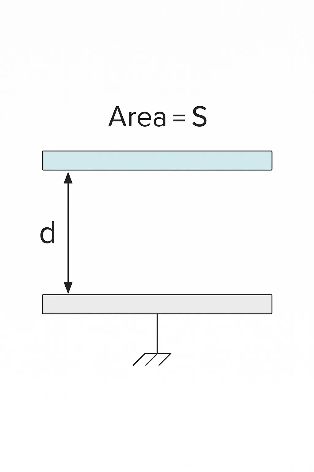
The capacitance between the body and ground is shown in Figure 2. The relative permittivity of the shoe sole, the sole area S, and the sole thickness d determine the sole contribution.
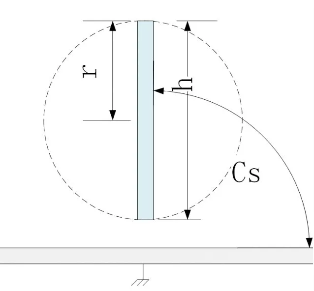
Viewing the human as an isolated conductor, the capacitance to free space is shown in Figure 3, where h is the body height and r is the equivalent radius, often taken as half the body height.
1.2 Measurement of Human Model Parameters
In 1976, Kocak et al. proposed a method using a high-voltage source and a 10 MΩ resistor to charge both the subject and a reference capacitor C = 2700 pF to a voltage V. The subject and the capacitor are then discharged to ground through a 1 kΩ resistor while the discharge current waveforms are captured with a current probe and an oscilloscope. By comparing peak discharge currents of the subject and the reference capacitor, the equivalent body resistance can be determined.
The capacitor discharge peak current is I0 = V / 1000, and the human discharge peak is Ip = V / (1000 + Rb), where Rb is the body equivalent resistance. From this, Rb = (V - 1000×Ip) / Ip = 1000(I0 - Ip) / Ip. After measuring I0 and Ip, Rb can be calculated.
By computing the time constant τ of the body discharge waveform and using τ / Rb, the body capacitance CB can be obtained. Values measured by this method are CB = 132–190 pF and RB = 87–190 Ω.
In May 1980, the U.S. Navy released the DOD1686 standard specifying a standard human ESD model using a 100 pF capacitor in series with a 1.5 kΩ resistor. Standards such as ESD STM5.1-1999 and IEC 61340-3-1 define the circuit parameters, discharge current waveforms, and current parameters for the standard human model.
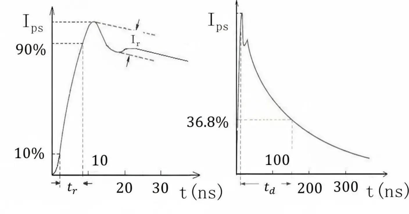
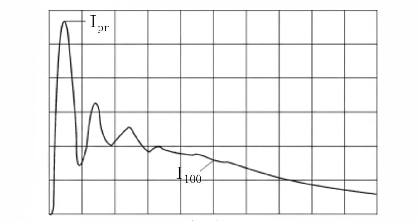
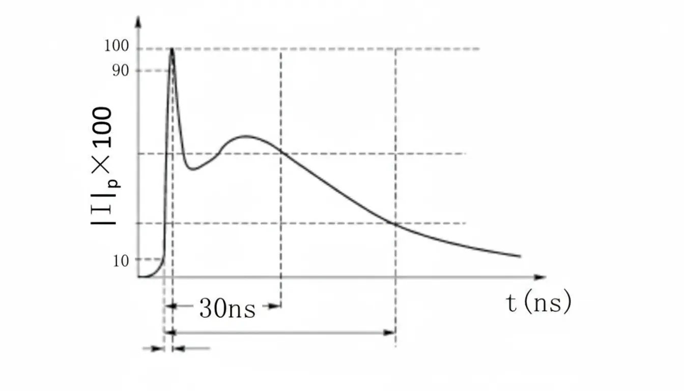
Figure 4 shows the short-circuit current waveform of an ESD model. Ir is the maximum oscillatory current peak-to-peak, less than 15% of the short-circuit discharge peak current Ips and should not be observable 100 ns after the pulse start. tr is the pulse rise time, typically 2–10 ns, and td is the pulse decay time, typically 150 ± 20 ns.
Note that standard human-model parameters are intended for sensitivity testing of devices or equipment in different situations; parameter values vary by test context.
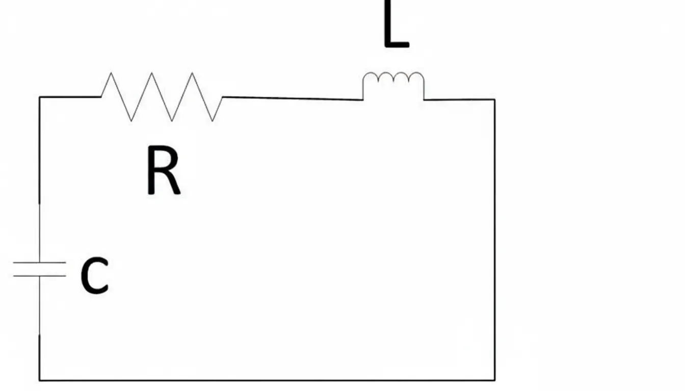
2. Machine Model
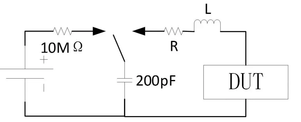
The machine model (Machine Model, MM) was first proposed in Japan to simulate discharge events from charged conductors to electronic devices. For example, in the SMT production stage, components may contact charged metal and suffer ESD damage. The equivalent circuit is shown in Figure 5, where R is the loop equivalent resistance and L is the loop equivalent inductance.
The machine model was initially intended to study a more severe case than the human model; thus its equivalent resistance R should be as small as possible, often taken as zero. The equivalent inductance is also very small and often approximated as zero. Comparative tests show the machine model is more severe than the human model: under the same voltage conditions, devices are generally more sensitive to the machine model.
Because achieving sufficiently low inductance in practical ESD simulators is difficult and vendor consistency varies, standards such as ESD STM5.2-1999 and IEC 61340-3-2 specify mechanical model waveforms. The short-circuit current waveform is shown in Figure 6, and the waveform when discharged through a 500 Ω resistor is shown in Figure 7.
Designers often focus on device HBM robustness while paying less attention to the machine model. One reason is a disconnect between R&D engineers and production processes in the Chinese market, so production-level ESD control capability may not be well understood. It is important to assess the SMT supplier and the ESD control capability of their equipment. When selecting components, ensure device robustness exceeds the ESD levels generated by production machinery and control each process step.
3. Charged-Device Model (CDM)
The charged-device model (Charged Device Model, CDM) describes the situation where devices themselves become charged during handling, processing, or transport through contact or friction with objects and packaging. When a charged device approaches or contacts a conductor, electrostatic discharge occurs. CDM discharges can cause significant damage to sensitive devices, and increasing pin counts on ICs have raised the risk of charged devices. The CDM was first proposed by Speckman et al. in 1974 and is shown in Figure 8.
In this model, C is the device-to-ground capacitance, typically a few pF depending on pin layout and package structure. R represents the resistance of the internal discharge path, usually a few ohms. Because R is small, equivalent inductance cannot be ignored, so the model includes an inductance L.
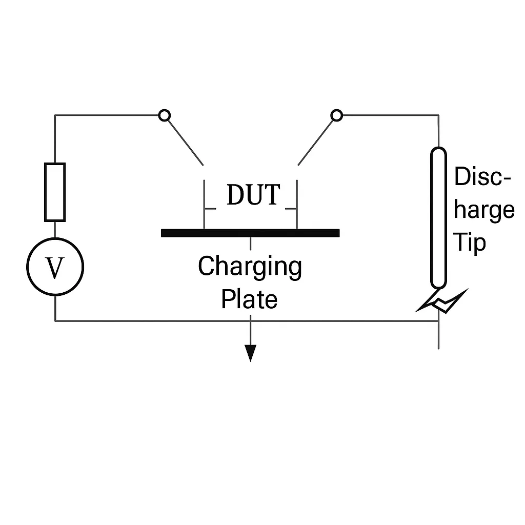
Two charging methods are commonly used to measure device robustness: direct contact charging and field-induced charging. Direct charging charges the DUT by physical contact; care is required because charging can damage the DUT. Field-induced charging uses an electric field to charge the DUT by induction, avoiding the risk of damage during charging. Field-induced charging is generally preferred for testing.
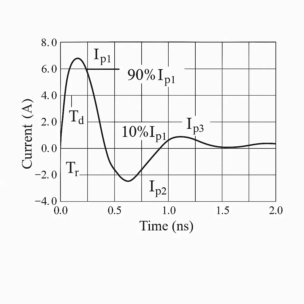
The ESD Association standard ESD STM5.3.1-1999 specifies CDM discharge waveforms, where Tr is less than 200 ps and Td is less than 400 ps.
Typical charged-device robustness for many electronic components is only a few hundred volts. During packaging, storage, and transportation, strict control of charge generation is essential; use antistatic materials for packaging. Observations from manufacturing show components sometimes shipped in small plastic bags rather than full reels, increasing ESD risk. This reflects a lack of understanding of charged-device mechanisms in some production environments; practical controls are necessary in addition to theoretical knowledge.
4. Transmission Line Pulse and Field-Induced Models
4.1 Transmission Line Pulse (TLP)
TLP testing provides information on possible device failure mechanisms. The TLP equivalent model is shown in Figure 12.
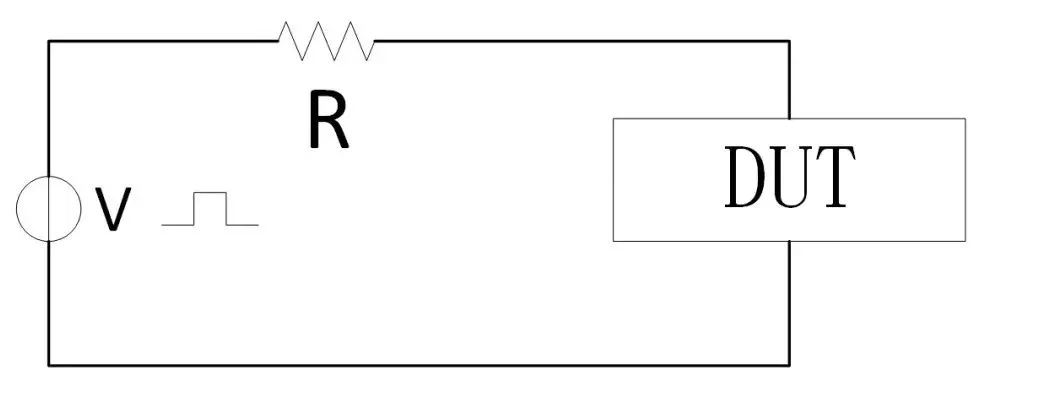
TLP test parameters are easy to control: a voltage square pulse of height V is applied, and the current is I = (V - Vdut) / R. Pulse duration depends on transmission length, t = 2(L/c), where c is the speed of light. By incrementally increasing pulse height V, a DUT I-V curve is obtained. Observing breakdown points and DC leakage avalanche thresholds allows assessment of ESD failure levels. Designers can analyze ESD robustness and protection strategies from the measured I-V curve.
4.2 Field-Induced Model
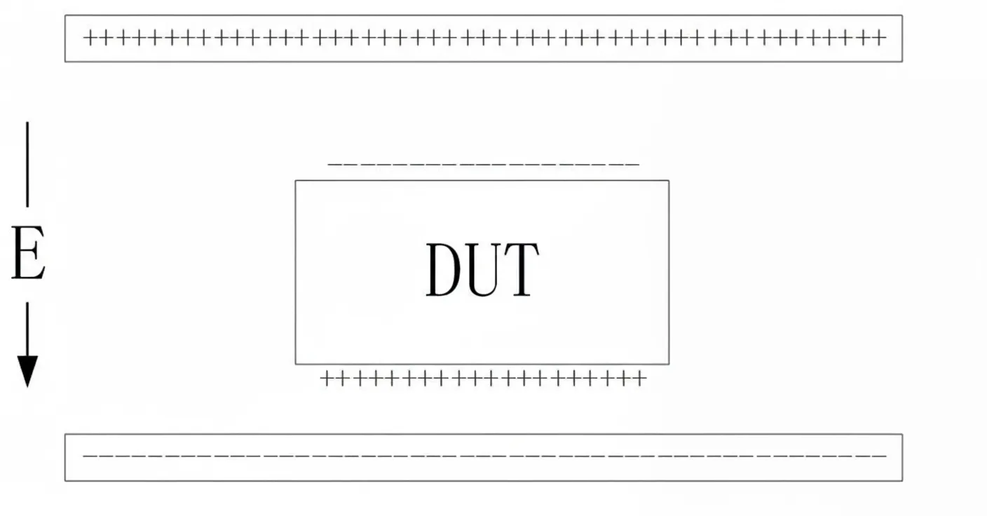
The field-induced model describes polarization or electrostatic induction when an insulated electronic device is in an electrostatic field. Charge separation on such objects can produce induced potentials that, if large enough, cause the device to discharge to surrounding conductors. This field-induced ESD mechanism indicates that devices should not be stored or used in strong electrostatic fields without appropriate protection. Equipment that must operate in strong fields requires adequate ESD mitigation.
5. Body-Metal Model
The body-metal model (BMM) simulates a charged person holding a small metal object such as a screwdriver or key discharging to another object. The metal object's tip effect amplifies local field strength and reduces equivalent discharge resistance, producing higher peak discharge currents and shorter durations than a naked-body discharge. The equivalent is shown in Figure 14.
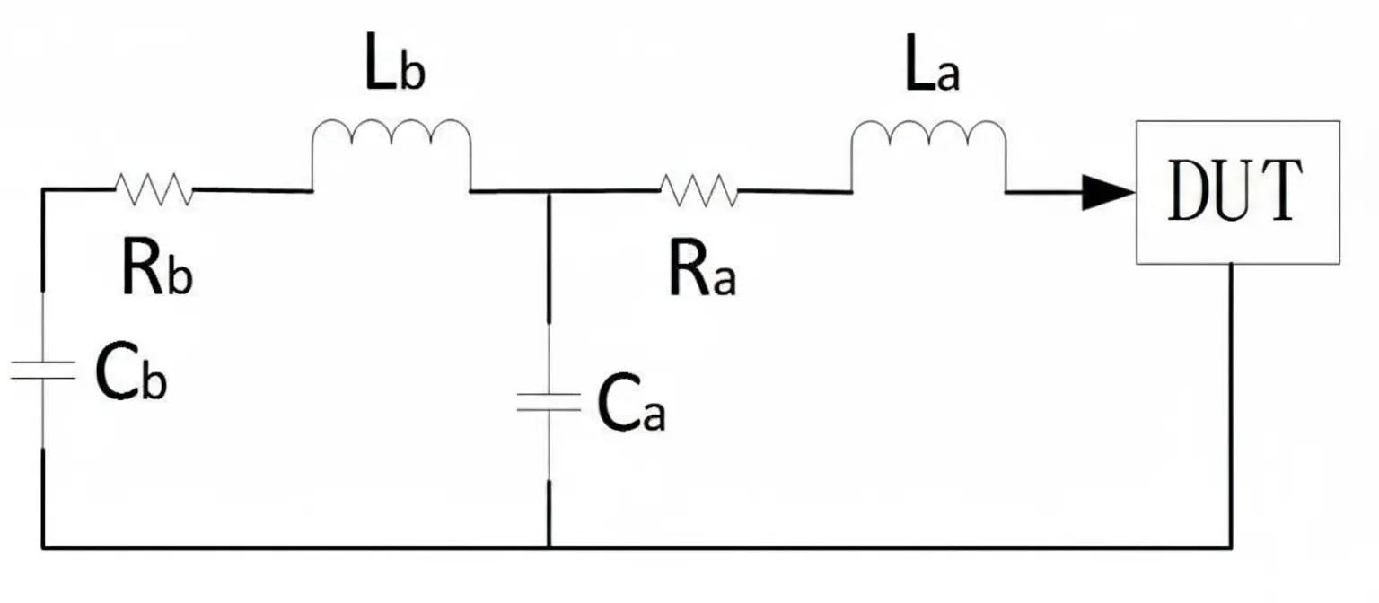
Cb is the body equivalent capacitance, Rb the body equivalent resistance, and Lb the body equivalent inductance. Ca, Ra, and La represent the equivalent capacitance, resistance, and inductance of the hand and the held metal object. IEC-1000-4-2 (equivalent to IEC 61000) specifies typical parameters: Cb = 150 pF ± 10%, Rb = 330 Ω ± 10%, Lb = 0.04–0.2 μH, Ca = 3–10 pF, Ra = 20–200 Ω, La = 0.05–0.2 μH.
The body-metal discharge waveform is shown in Figure 15. The body-metal model has a faster rise time, about 0.7–1 ns, compared to the HBM rise time of 2–10 ns. The faster rise is mainly due to a very small, nearly noninductive capacitance Ca between the hand and the metal object, leading to a steeper edge during discharge.
6. Furniture Electrostatic Model
The furniture electrostatic model covers movable furniture in data centers or labs, such as chairs and small carts, which can become charged by friction or induction and discharge to nearby equipment. IBM conducted some of the early research on furniture ESD. They compared human ESD, body-metal ESD, and furniture ESD and found that, at the same discharge potential, furniture ESD can produce higher peak currents and therefore greater hazard. The equivalent model is shown in Figure 16.
European computer manufacturers' standards include the furniture model, while IEC includes only the body-metal model. China’s standards typically reference IEC, so the furniture model is not commonly used in those standards.
7. IC-Related ESD Models
7.1 Charged Chip Model (CCM)
The charged chip model simulates ESD damage that can occur during wafer handling, such as when a chip on an insulating film is picked up with a metal tweezer during assembly. Static charges on the insulating film can put the chip at high potential. When the charged chip discharges to the metal pickup, a fast-rising transient current flows into the chip through the metal tool, imposing transient high voltages on internal structures and potentially causing damage. CCM is used to test wafer-level ESD sensitivity, as shown in Figure 18.
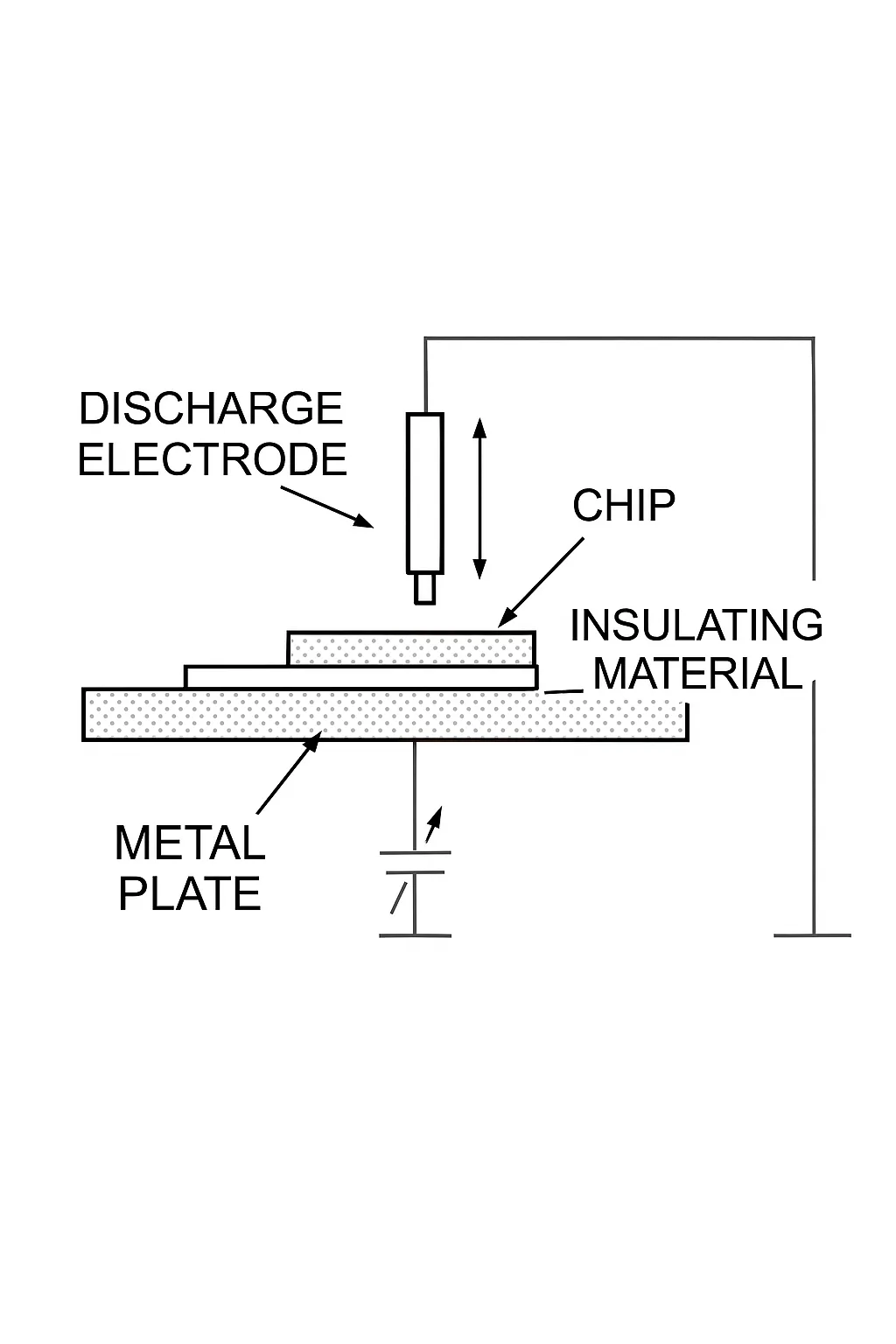
7.2 Charged Package Model (CPM)
Charged package model testing differs from CDM by removing humidity influence. Under high humidity, CDM results can depend on the time between charge and discharge. CPM ensures all device pins are charged simultaneously through a high-resistance material, such as phenolic plastic. When a discharge electrode approaches the DUT, the device discharges through a grounded 1 Ω resistor and the waveform is observed with an oscilloscope. Prior to the next charge, electrodes neutralize the connectors so residual charge leaks to ground through 1 MΩ resistors. CPM charging methods aim to better reproduce actual charging seen in real-world handling.
7.3 Charged Board Model (CBM)
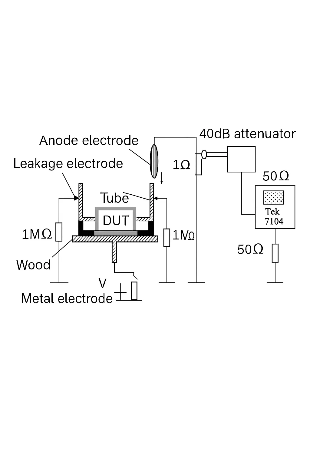
There has been misunderstanding about PCB-level ESD, with assumptions that PCB-mounted components are protected. Many observations show that ESD voltages that damage components on a PCB can be lower than those measured in component-level CDM or HBM tests.
In CBM tests, the PCB under test is placed on an insulating board supported by grounded metal. The PCB is charged from a high-voltage source and discharged to ground through a connector and a 1 Ω resistor. Failures on the PCB typically occur in two common scenarios: first, a charged person touches a circuit board that is directly or capacitively grounded; second, a person carrying a charged board causes a discharge when the board contacts metal supports and the charge quickly leaks to ground, producing an ESD event.
EMC Remediation Tips
1. Differential-Mode and Common-Mode Noise
Difference between the two:
Differential-mode noise: Exists between the L and N lines. Current flows from L through the rectifier diode anode, through the load, via return ground, and back to N. High-speed switching devices and diodes with very short reverse-recovery times generate high-frequency noise that flows through this loop and can be detected by measurement receivers, causing conducted emissions failures.
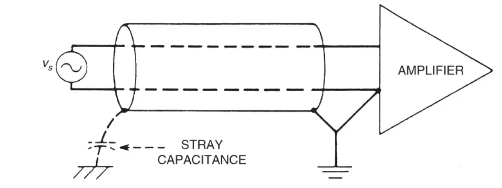
Common-mode noise: Results from parasitic capacitance between the equipment and earth. High-frequency noise couples through this parasitic capacitance and creates common-mode currents between earth and the cable, causing common-mode interference.
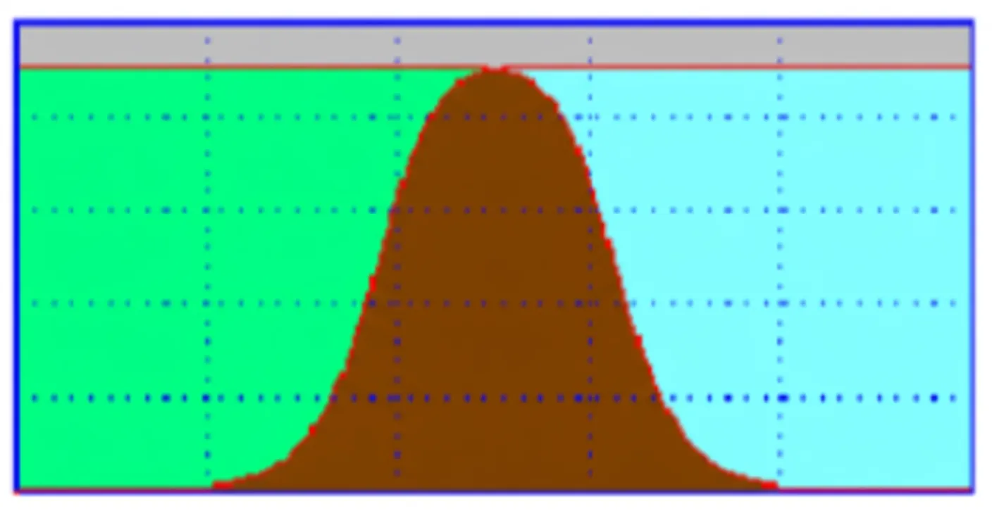
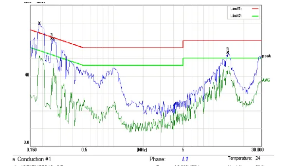
Figure shows conducted FALL data caused by differential-mode noise; the front-end is out of limit due to differential-mode interference.
The following diagram illustrates the EMI principles of a switch-mode power supply:
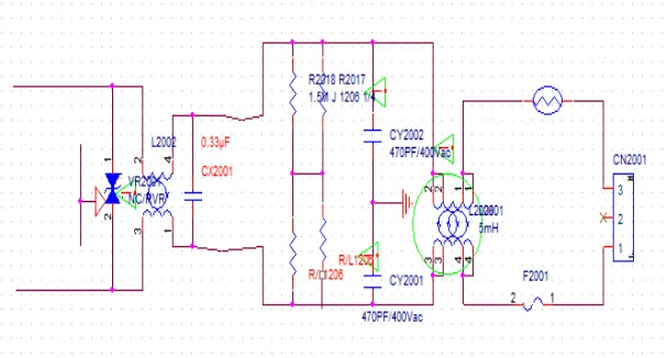
In the diagram, CX2001 is an X-rated safety film capacitor across L and N. When current flows through the load between L and N, it carries high-frequency noise. The X capacitor provides a local loop between the load and the capacitor so high-frequency components are shunted and dissipated locally rather than being injected back to the mains.
Countermeasures for differential-mode noise:
- Increase the value of the X-class capacitor.
- Increase the differential leakage inductance of common-mode chokes to utilize leakage inductance and suppress differential-mode noise. In practice, imperfect winding tightness and length differences produce leakage flux, creating an effective series inductance between L and N that helps attenuate differential noise.
Parasitic capacitance between the power cable and earth forms a return path for common-mode noise. The noise flows through the cable-earth parasitic capacitance to earth, forming a common-mode current that is detected by the LISN and the measurement receiver, potentially causing conducted emissions failures. This also explains why some motherboards pass conducted tests when not grounded but fail once a ground clip is attached. In USB mode without earth, the return loop is L → diode → load → chassis ground → diode → N, and common-mode current cannot return to the LISN, so detected noise is smaller. When the board chassis is connected to earth, the cable-earth parasitic capacitance creates a loop and, if common-mode noise is not sufficiently absorbed by the front-end LC filters, conducted limits can be exceeded.
Countermeasures for common-mode noise:
- Increase the common-mode choke inductance.
- Tune LC filters on L-GND and N-GND to reject common-mode noise.
- Ensure the mainboard is properly grounded to reduce earth impedance and minimize the cable-to-earth parasitic capacitance effect.
2. Common EMI Sources
Examples of common electromagnetic interference sources include:
- Switch-mode power supply switching loops: fundamental frequencies from tens of kHz to a few hundred kHz; harmonics extend into tens of MHz.
- DC power rectifier circuits: linear mains supplies produce rectifier noise up to several hundred kHz; switch-mode supplies produce rectifier noise extending into tens of MHz.
- Brush noise from DC motors: noise can extend up to several hundred MHz.
- AC motor operating noise: higher harmonics can extend into tens of MHz.
- Variable-frequency drive circuits: switching frequencies range from tens of kHz to tens of MHz.
- Switching noise from changeovers: mechanical or electronic switching can produce noise up to several hundred MHz.
- Clock oscillators and digital circuits in smart control equipment: fundamental frequencies from tens of kHz to tens of MHz; harmonics can extend into hundreds of MHz.
- Microwave equipment leakage: main frequencies in the GHz range.
- Electromagnetic induction heating equipment: fundamentals in tens of kHz; harmonics extend into tens of MHz.
- TV tuner local oscillators and harmonics: tens to hundreds of MHz; harmonics can reach GHz.
- ICT and control equipment digital processing circuits: fundamentals in tens to hundreds of MHz; internal multiplication can produce GHz-level signals and harmonics extending to tens of GHz.