ALLPCB


Overview
EMC design is a common challenge for electronic engineers. Electromagnetic compatibility (EMC) refers to a device or system's ability to operate acceptably in its electromagnetic environment and not generate electromagnetic interference that is intolerable to other equipment in that environment. EMC thus has two requirements: one is that emissions generated during normal operation must not exceed specified limits; the other is that the device must have a certain degree of immunity to electromagnetic disturbances present in its environment. Electromagnetic interference (EMI) refers to any electromagnetic phenomenon that degrades the performance of a device or system.
EMI and EMS
EMC comprises two parts: EMI (electromagnetic interference) and EMS (electromagnetic susceptibility/immunity). EMI denotes the unwanted electromagnetic noise produced by a device while performing its intended function that adversely affects other systems. EMS denotes the device's ability to perform its intended function without being adversely affected by the surrounding electromagnetic environment.
Design Considerations
To achieve good EMC performance at acceptable cost, EMC must be addressed during product design. EMC performance is determined by design; testing only quantitatively characterizes the product's inherent EMC behavior. Key points for EMC design include:
First, consider EMC early in the development process. If EMC issues are ignored until the testing phase and are treated only by rework, a large amount of human and material resources will be consumed during verification and remediation. Even if remediation succeeds, changes to circuit schematics, PCB layout, or mechanical tooling often substantially increase development cost and time. Only by predicting and controlling EMC issues during early design, and running EMC considerations in parallel with functional design, can the product be done right the first time.
Second, perform EMC design systematically. Improving EMC performance through design cannot rest on a single EMC specialist, because EMC cannot be separated from hardware, mechanical structure, and other physical aspects of the product. Achieving acceptable EMC performance at first pass requires raising EMC awareness and experience across the engineering team.
Roles and Responsibilities
Hardware engineers should, beyond core circuit design knowledge, understand basic EMI and EMS mitigation techniques. PCB designers should be familiar with component placement, layer stackup, and high-speed routing practices that affect EMC. Mechanical or enclosure engineers should understand shielding and grounding design principles. Engineers involved in product design must comprehend and apply EMC recommendations from specialists, integrating those measures with domain-specific constraints to eliminate EMC issues during design. Only when all developers improve their EMC competence can products achieve high EMC performance.
Neglecting EMC during design commonly leads to test failures and inability to meet regulatory requirements.
Trends Increasing EMI Concern
As electrical and electronic technologies develop and consumer electronic products become more widespread and feature-rich, and with the growth of broadcast, telecommunications, computing and networks, the electromagnetic environment has become more complex and challenging. EMI and EMC issues are therefore receiving increasing attention from engineers and manufacturers.
ESD Protection
ESD protection can be broadly divided into two categories:
- Conductive ESD protection. To protect circuits from electrostatic discharge currents, protective components are typically placed at the front end of sensitive devices to divert or dissipate the current. Typical components include ceramic capacitors, varistors, and TVS diodes.
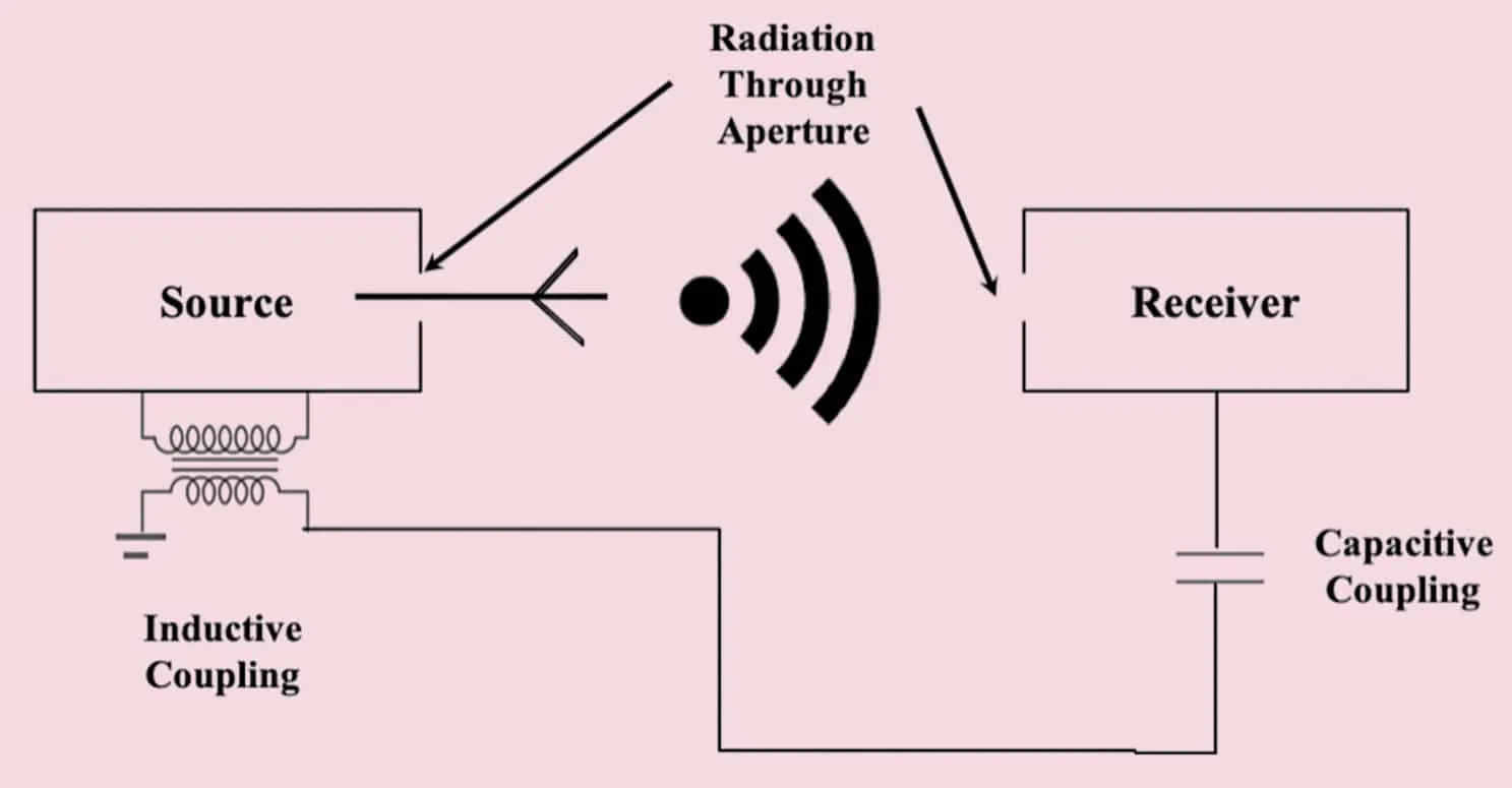
- Radiative ESD protection. When an electrostatic field affects sensitive circuits, protection focuses on reducing field generation and energy, improving structural design to increase protection, and shielding sensitive traces. Field-based protection is generally more difficult. One practical method is equipotential bonding: effectively connecting conductive parts so the enclosure forms an equipotential body, which suppresses discharges. This method has proven effective and is straightforward to implement.
General Static Protection Methods
Common methods to protect against static include reducing charge accumulation; insulating product surfaces to prevent discharge; providing shunt paths to divert static currents away from sensitive traces; shielding circuits in discharge-prone areas; and minimizing loop areas to reduce susceptibility to magnetic fields generated by ESD events. Protective measures can target direct discharge as well as coupled fields.