ALLPCB


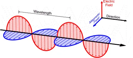
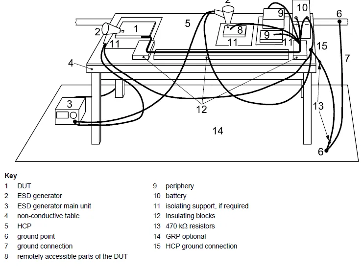
ESD is classified into contact discharge and air discharge, with air discharge typically representing higher energy. Below is the ISO 10605-2008 ESD test setup. The following protection methods are summarized for reference in product design.
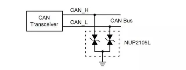
1. TVS diodes
TVS diodes are commonly placed at ports such as low-speed signal lines, high-speed signal lines, and RF antenna ports. The avalanche breakdown of a TVS clamps the voltage and protects downstream circuitry.
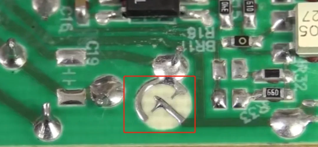
2. MLCC ceramic capacitors
For cost-sensitive products, MLCC capacitors are typically placed at I/O connectors or critical signal points. Keep the connection leads as short as possible to reduce lead inductance.
3. Spark gap method (not recommended)
The spark gap produces an arc for ESD discharge (similar to tracking; effectiveness drops if the gap is too large), discharging via a sharp tip to ground to dissipate energy. This method is prone to carbon tracking and has a limited service life, so it is generally not recommended.
4. Metal shielding
When electrostatic currents flow through metal conductors, parasitic inductance at high frequencies creates changing electromagnetic fields on the conductor. If sensitive signals are close to a metal backplane, induced interference voltages can appear on signal traces and cause system malfunction. Shielding can mitigate this effect.
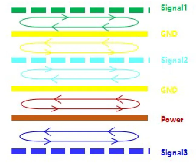
5. PCB stackup design
The key principles for PCB stackup are that high-frequency signals have a continuous reference plane and minimal loop area. Placing the power plane adjacent to the reference plane provides a fast current return, and minimizing loop area reduces the susceptibility to induced currents.
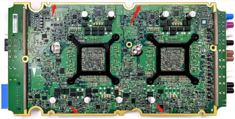
6. PCB anti-static perimeter ring
Route a solder-mask-free trace around the PCB perimeter and, where practical, connect this trace to the enclosure. Include a gap in the ring to avoid creating an antenna. This anti-static ring is commonly used in automotive domain controllers; the exposed copper around the PCB perimeter forms the anti-static ring.
7. Grounding and bonding
Grounding and bonding provide low-impedance paths for electrostatic currents. Good bonding between metal parts establishes low-resistance current paths and reduces parasitic inductance between different reference planes, helping to maintain equipotential reference planes across operating frequencies.
Summary: Protecting the circuit power and signal lines effectively reduces the likelihood of ESD currents entering the PCB.