ALLPCB


1. Overview
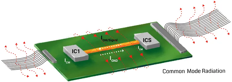
Multilayer printed circuit boards should be designed for electromagnetic compatibility (EMC) so that the board meets emission and susceptibility standards during normal operation. A correct stackup helps to shield and suppress EMI.
2. Fundamentals of Multilayer PCB Design
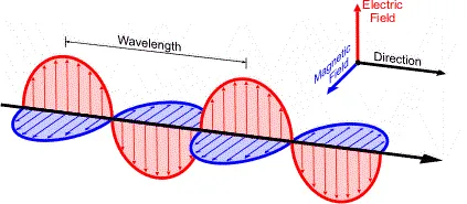
EMC analysis for multilayer PCBs is based on Kirchhoff's laws and Faraday's law of electromagnetic induction.
From these principles, the following basic guidelines for PCB layering and stackup can be derived:
- Power planes should be placed as close as possible to ground planes, and should be positioned adjacent to a ground plane.
- Signal routing layers should be placed adjacent to their reference plane layers.
- Power and ground plane impedance: the power-plane impedance Z0 depends on the spacing between the power and ground planes (D) and the area of the planes (W).
- Trace geometry differs by layer: internal layers form stripline while outer layers form microstrip; their characteristics differ.
- Critical signals should be routed immediately adjacent to a ground plane.
3. PCB Stackups and Layering
2-layer boards
Two-layer boards are suitable only for low-speed designs and generally have poor EMC performance.
4-layer boards
Common 4-layer stackup variants are described below. Notation: S1 = signal layer 1, S2 = signal layer 2, GND = ground plane, POWER = power plane.
Configuration A: One common approach places a ground plane on the outer layer for EMI shielding, with the power plane close to ground to minimize power-plane impedance. This configuration is not ideal for boards with high routing density because it can compromise ground plane integrity and degrade performance for the second signal layer. It is also not suitable for boards with high board-wide power dissipation.
Configuration B: A frequently used arrangement but not ideal for high-speed digital designs because it is difficult to maintain low power-plane impedance. For example, for a 2 mm total board thickness aiming for Z0 = 50 ohm with an 8 mil trace width and 35um copper, the gap between signal layer 1 and the ground plane is about 0.14 mm, while the gap between the ground and power planes is about 1.58 mm, which substantially increases power-plane impedance. Radiation from this stackup tends to be into free space and may require shielding to reduce EMI.
Configuration C: Signal quality on S1 is best, S2 is second. This provides some EMI shielding but has higher power-plane impedance. This stackup can be used when the board has high overall power dissipation and is the source of interference or is adjacent to an interference source.
6-layer boards
Configuration A: Common arrangement; S1 is a good routing layer, S2 is secondary. Power-plane impedance is relatively poor; routing should consider the interaction between S2 and S3.
Configuration B: S2 is a preferred routing layer and S3 is secondary; power-plane impedance is improved.
Configuration C: S1, S2, and S3 are all good routing layers and power-plane impedance is acceptable. The trade-off is one fewer routing layer compared with some other arrangements.
Configuration D: Offers better overall performance than the first three in some respects, but has fewer routing layers. This layout is often used for backplanes.
8-layer boards
For an 8-layer board with six signal layers, layout A is an option, though it is not ideal for high-speed digital designs. For five signal layers, layout C is preferred; S1, S2, and S3 are good routing layers and the power-plane impedance is relatively low. For four signal layers, the option corresponding to table B makes each signal layer a good routing layer. In all these cases, adjacent signal layers should be routed with consideration of their reference planes.
10-layer boards
For 10-layer boards with six signal layers there are several stackup choices; configurations A and C usually perform better than B. In A, S1 and S6 are excellent routing layers; S2, S3, and S5 are secondary. A is generally better than C because in C the distance between GND and POWER is determined by the spacing to S5, which may not guarantee low power-plane impedance.
Configuration D is a balanced 10-layer stackup where each signal layer is a good routing layer. Configurations E and F are often used for backplanes; F provides better EMC shielding than E. A potential downside is where two signal layers are adjacent, routing between them requires attention.
In summary, PCB layering and stackup design is complex and depends on multiple factors. Focus on the required functions and the key constraints of your design to determine an appropriate stackup.