ALLPCB


Overview
As software-defined radio (SDR) platforms have appeared in military, aerospace and some consumer radio and electronics applications, field-programmable gate arrays (FPGAs) have become increasingly important as reconfigurable engines for digital signal processing (DSP) in SDR systems.
FPGA as an Interface to High-Speed Peripherals
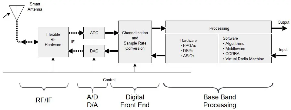
Field-programmable logic commonly serves as the interface between wideband A/D and D/A converters, digital receivers and communication links and the programmable processors in embedded real-time systems. FPGAs are well suited to handling clocking, synchronization and other timing circuits needed to tame these specialized devices. They are also effective for data-formatting tasks such as serial-parallel conversion, data packing, timestamping, multiplexing and packet formation.
FPGA DSP Capabilities
FPGA vendors have invested heavily in DSP capabilities over recent years. Gate densities have followed Moore's law, roughly doubling every 18 months, and some recent devices claim millions of gates. Modern FPGAs are built from logic cells that include memory and can perform arithmetic functions. High-density logic now supports fast multipliers, block memory for FFT processing and distributed memory for FIR filtering.
Synthesis tools now support parameterized cores that accept bit-width definitions and generate structures to meet signal-processing precision without wasting logic. A variety of front-end design tools cater to different engineering preferences, including system-level block diagrams, schematic capture and HDL compilers for Verilog and VHDL. Improved analog simulators simplify verification and reduce debug time.
Third-party IP vendors supply cores that complement vendor-supplied libraries, ranging from full DSP processors to application-specific modules such as high-speed modem blocks. With these commercial building blocks, FPGAs can address markets traditionally served by ASICs and DSPs. Because FPGAs can integrate many parallel multiply-accumulate units, they often outperform general-purpose DSPs on algorithms that require high multiply parallelism.
DSP Tasks in Software Radios
In a typical SDR receiver, filtered baseband signals from A/D converters are delivered to a DSP as a complex sample stream. The DSP handles demodulation and higher-level signal analysis. Intelligent receivers may classify modulation by spectral analysis, then apply demodulation algorithms to determine whether useful information such as intelligible voice or meaningful data is present. Other DSP tasks include decryption, data storage, channel switching, routing to other systems, activity logging and presenting audio or digital data to operators.
In cellular base stations, the number of DSP tasks grows with each new communication standard. The proliferation of complex digital voice and data protocols increases the need for decoding, convolution, framing, error correction and vocoding. Rising sampling rates further increase processing load and push DSP resources closer to the antenna. To meet these demands, DSP clock rates have exceeded 200 MHz and many devices include multiple hardware multipliers, but minimizing the workload on these relatively costly and power-hungry processors remains important.
FPGA Roles in SDR
Over the past five years FPGAs have advanced in several key areas to address DSP functions. High-density devices now provide abundant logic, block RAM and dedicated multipliers. These resources support fast multiplier arrays, block memory for FFTs and distributed memory for FIR filters. The ability to reconfigure hardware without new board designs makes FPGA-based commercial off-the-shelf (COTS) boards attractive for SDR systems: the same hardware can be repurposed for future applications by loading new FPGA designs.
New algorithms can be prototyped on DSPs using code generation, simulation and optimization tools, then migrated to FPGAs for improved real-time performance or parallel channel processing. For production, many FPGA designs can be converted to custom ASIC masks if required.
Example: SDR Module with FPGA and DSP
An illustrative example is a dual-channel digital receiver daughtercard connected to a quad-DSP VME board. The daughtercard includes two 12-bit A/D converters capable of sampling up to 100 MHz and two digital downconverters for selecting and filtering wideband digitized inputs.
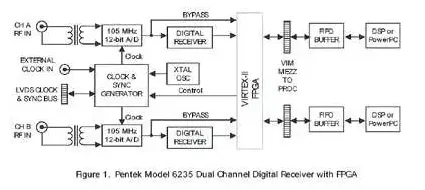
The onboard FPGA accepts the two A/D outputs and the complex baseband outputs from the downconverters. The FPGA implements a VIM-style interface to transfer data directly to each DSP or PowerPC on the processor board, with FIFO buffers supporting DMA block transfers at rates up to 400 MB/s.
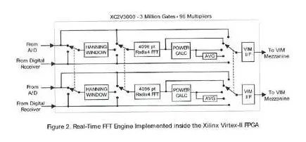
For DSP augmentation, a natural FPGA choice for this platform is the Xilinx Virtex-II family. The XC2V3000 provides 96 dedicated 18x18 multipliers and over 200 KB of block RAM, offering a rich combination of signal-processing resources. In the module's baseline factory configuration, the FPGA handles timing, formatting and glue logic and uses only 6% of the programmable logic, leaving most logic, all 96 multipliers and most block RAM available for DSP algorithms.
Implementing a High-Performance FFT
To demonstrate available resources, an engineering project implemented a high-performance FFT engine. FFTs remain a key benchmark for processors because communications, radar and signal-intelligence systems use them for tracking, tuning and image processing. A FFT accepts a block of time-domain samples and converts them to frequency-domain samples; the computation is intensive and consumes substantial DSP resources, making it a prime candidate for FPGA implementation.
One efficient FFT method uses an iterative radix-4 butterfly algorithm. Each butterfly multiplies four input data points by sine/cosine coefficients and combines them to produce four output points. Repeating the butterfly stages processes the entire input. A 4,096-point FFT requires six butterfly stages. Unlike a conventional processor, an FPGA can perform many multiplications in parallel. In the 4,096-point example, 60 multipliers are required to implement all six FFT stages in parallel. With 96 available multipliers on the XC2V3000, the FPGA can outperform DSPs that typically offer only two or four multipliers.
FFT efficiency requires random access to memory for inputs and outputs. A/D converters supply sequential samples, so the FPGA uses configurable block RAM to reshape memory into a structure that feeds the butterfly engine with parallel samples via four memory ports. This custom memory architecture allows continuous pipelined processing of input blocks so that multipliers in all six stages remain efficiently utilized.
Each FPGA clock cycle, a radix-4 butterfly processes four input samples. When the FPGA clock equals the A/D clock, the architecture can run four times faster than real time. With suitable hardware multiplexing, a single FFT engine can serve four input streams instead of one. In the example, both the two A/D converters and the FPGA run at 100 MHz, so the FPGA initially runs at half capacity. By introducing 50% input overlap processing, the engine can be configured to fully utilize the hardware. In that case each FFT pipeline completes in 10.24 microseconds, four times faster than the time required to collect 4,096 samples at 100 MHz, consistent with real-time execution of four FFTs.
FFT Enhancements
Of the 96 multipliers, only 60 are required for the FFT core, leaving room for additional functions. Optional Hanning windows can be applied to each of the four complex input streams, consuming eight additional multipliers. Because the FFT and window coefficients are stored in separate FPGA table memory, alternative window functions can be substituted. Another eight multipliers can be used to compute output power: squaring the real and imaginary parts of each of the four outputs and summing them. An averaging stage combines the outputs from overlapping FFTs to improve signal-to-noise characteristics.
Muxing at the FPGA output permits routing results from each signal-processing stage to the processor interface. The figure below shows the FPGA internal blocks used on the module described above.
Conclusion
The implemented FPGA FFT engine executes a 4,096-point complex FFT in 10.24 microseconds, about ten times faster than an optimized FFT benchmark on a 400 MHz G4 PowerPC. Techniques to reduce rounding and truncation errors in integer FPGA arithmetic enable computed dynamic ranges in excess of 90 dB. After optimizing for speed, the design used 76 of the XC2V3000's 96 multipliers, 99% of logic slices and 97% of block RAM. While this specific FPGA component is relatively costly, the family includes smaller devices with compatible package pinouts that can reduce cost for less-demanding applications.