ALLPCB


Scan and BIST are two DFT techniques. They involve adding hardware to a chip specifically for testing; they are not part of the functional logic.
Scan Design — scan path design
Scan techniques were first proposed by Kobayashi and others. The basic idea is that sequential circuits can be modeled as a combinational network. The primary goal of scan design is to improve controllability and observability.
By inserting additional hardware between logic A and logic B, the value propagated from logic A to logic B can be observed and controlled.
Scan process
Scan is typically applied in two steps.
1. Scan replacement
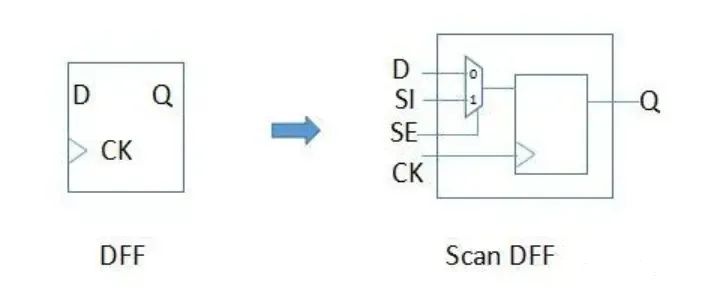
Replace standard D flip-flops with scan DFFs. The figure below shows a mux-D type DFF: it adds SI, SE, and a mux.
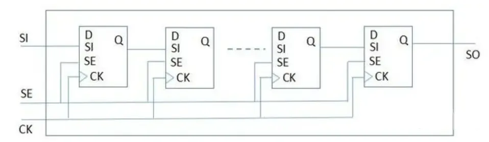
2. Scan stitching
Scan stitching connects the Q and SI of the scan DFFs obtained in the previous step to form scan chains. At the chip top level there is typically a global SE signal and scan chain input/output signals: SI and SO. By operating the scan chain sequentially, testing of complex sequential circuits can be reduced to testing combinational logic.
The previous diagrams showed only sequential elements; the combination with combinational logic forms the full design under test.
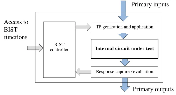
BIST — built-in self test
Built-in self test (BIST) is a design technique that adds test circuitry to the chip. During test, only external control signals are required to run the on-chip test hardware and software to check for faults. Unlike scan-based testing, BIST test vectors are typically generated internally rather than supplied externally. BIST can simplify test procedures and reduce dependence on expensive external test equipment such as ATE, but it increases design complexity.
BIST is generally classified into Logic BIST (LBIST) and Memory BIST (MBIST).
LBIST is used for testing random logic. It typically uses a pseudorandom pattern generator to create input test patterns and a multiple-input signature register (MISR) to compact and capture output responses. MBIST is dedicated to memory testing; a typical MBIST includes test circuitry for loading, reading, and comparing test patterns. Industry-standard MBIST algorithms include March, March-C, and MATS+.
A related type, Array BIST, targets on-chip embedded memories. Analog BIST is used for testing analog circuits. BIST techniques are increasingly used as a complement to costly ATE solutions, though BIST does not currently replace external test equipment entirely and both approaches are likely to coexist.
Summary
Scan and BIST are two important techniques in chip testability design and are core skills for DFT engineers.