ALLPCB


Doherty amplifiers are used in many RF power applications. Although reference designs are often used, understanding their operation and the RF circuit design challenges is necessary to customize designs to meet specific requirements.
Designing a Doherty amplifier requires two amplifiers optimized for efficient operation, and the splitting, matching, combining, and phase must all be optimized to achieve the desired results and improve efficiency.
Starting an RF circuit design for a Doherty amplifier from scratch is a complex process that requires deep understanding of the technology and the performance of each amplifier component.
How a Doherty Amplifier Works
Before discussing RF circuit design for Doherty amplifiers, it is helpful to review basic RF amplifier operation.
The basic concept of the Doherty amplifier
The RF circuit of a Doherty amplifier uses a main amplifier, often called the carrier amplifier, which is typically biased to operate in class AB. The second active device, commonly called the peaking amplifier, is usually biased in class C.
The input signal is presented to the Doherty power amplifier and delivered to a splitter. This produces two signals that are shifted 90 degrees relative to each other. The 90 degree phase shift is produced by using an inductive splitter to reduce power loss while creating the required quadrature relationship between the two signals.
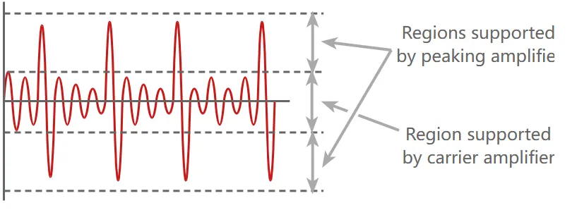
Operating regions of the Doherty amplifier
The signal is also presented to the peaking amplifier. That amplifier is biased so that it only begins to conduct when large peaks occur that the carrier amplifier cannot accommodate on its own. Because the peaking amplifier provides higher power only at higher power levels and is inefficient at lower power, it operates only when higher power is present. This arrangement yields improved efficiency across a range of output power.
After amplification, the signals are recombined by the combiner network at the output. The combiner also provides a 90 degree phase shift to cancel the input splitter's 90 degree shift, so that signals from the two amplifier paths arrive in phase at the load.
Operation Details
The basic Doherty theory requires the signals from the two halves to be phase-aligned at the combiner so that the outputs add constructively to produce the desired output.
Input power division is achieved with a quadrature splitter: common topologies include Lange or branch-line couplers.
The input behaves somewhat like a balanced amplifier. If the reflection coefficients of the amplifiers are equal in magnitude and phase, mismatches are reduced. Reflected waves are dissipated in the isolation port load of the coupler.
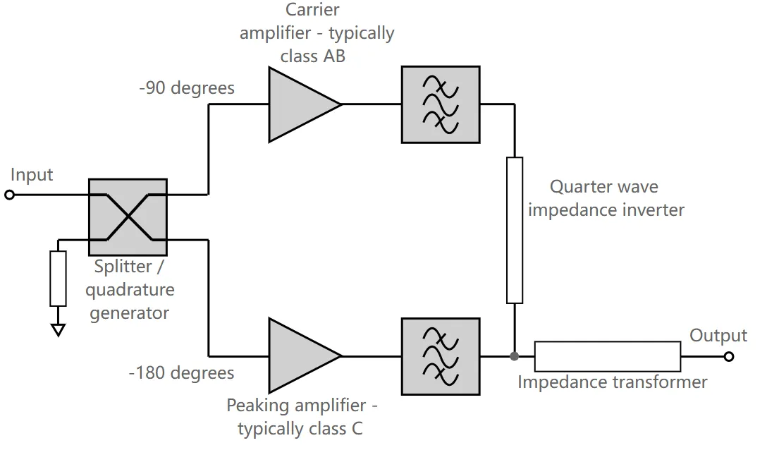
Doherty amplifier circuit blocks
Combining the outputs of the two amplifiers introduces additional challenges. Because the two signals are 90 degrees apart, a quarter-wave transmission line in the peaking amplifier output path is used to bring them back into phase at the combiner.
Impedances also must be matched precisely to maintain efficiency. Each RF amplifier presents an impedance of Z0/2, which is transformed to Z0 by a quarter-wave transformer.
Although this appears straightforward, the peaking amplifier operates only at peaks and therefore the amplifiers operate nonlinearly. During operation, one amplifier's response actively pulls the other amplifier's load due to their interaction, since they are not isolated. Nonlinear analysis is therefore required to complete the design.
Both RF amplifier sections can be biased to operate in the same class with adaptive bias schemes used to bring the peaking amplifier on line when required. Typically the carrier amplifier operates in class A or AB, and the peaking amplifier operates in class C. Alternative approaches include using devices of different sizes or using unequal power division at the input.
Design Challenges
In RF circuit design the goal is to deliver the best performance with the highest possible efficiency under expected conditions. These goals cannot all be achieved simultaneously, so significant trade-offs are required.
Achieving optimal overall performance requires finding a set of parameters and operating point that provide a good compromise between sensitivity to frequency, phase, and amplitude variations. This demands detailed knowledge of the amplifiers, splitter, and combiner characteristics.
Typically RF design practice involves starting from a vendor reference design and then tuning it. It is often difficult to fully optimize such designs for a specific application because only small changes are made to reference designs.
When designing a Doherty amplifier RF circuit, several interesting and challenging aspects must be addressed:
- Phase maintenance: Theoretically, signals arriving at the combiner via different paths should have identical phase. The RF splitter introduces a 90 degree shift in one leg that can be canceled at the combiner, since the combiner also induces 90 degrees and additional phase can be added in the other leg. However, the amplifiers introduce phase shifts that may not match, as one is designed to handle lower power levels and the other is designed for peaks. Their characteristics therefore differ, particularly in asymmetric designs.
- Impedance matching: Ensuring that the impedances of both RF amplifiers are well maintained across the operating range can be challenging in some designs. Optimizing various circuit elements to achieve this can be difficult.
- Maintaining linearity: Linearity can be disturbed when the peaking amplifier begins to conduct. This can increase distortion. Careful design is required to maintain linearity across the operating range.
- Bandwidth: Doherty designs are often bandwidth-limited. Some components, including splitters and combiners, have limited bandwidth and their phase responses vary, which affects overall amplifier performance.
In many cases, a Doherty amplifier reference design is used and only small component value adjustments are required. These reference designs are usually intended for common end uses, minimizing the need for extensive redesign.
Reference RF designs, including PCB layouts, can often be integrated into the overall printed circuit board layout with minor component value changes. Even so, care must be taken to ensure the final RF circuit performs as required. Small changes to the PCB layout can have a significant impact on performance.
Despite the RF design challenges, Doherty amplifiers have established a solid position in final power stages for cellular base stations and other wireless communications applications.
When the RF design is optimized, Doherty amplifiers can provide significant improvements in efficiency and related performance areas, which is useful in developing new cellular base stations, wireless systems, and other radio communication systems.